Crack DSP MCU TMS320F28035 Eeprom Memory
The TMS320F28035 devices use an advanced Harvard-type architecture that maximizes processing power by maintaining two separate memory bus structures in the process of Crack DSP MCU TMS320F28035 Eeprom Memory program and data — for full-speed execution. This multiple bus structure allows data and instructions to be read simultaneously.
Crack DSP MCU TMS320F28035 Eeprom Memory
Instructions support data transfers between program memory and data memory. This architecture permits coefficients that are stored in program memory to be read in RAM, thereby eliminating the need for a separate coefficient that are ROM by Dump NXP P89V52X2 Embedded Firmware. This, coupled with a four-deep pipeline, allows the ’x240 devices to execute most instructions in a single cycle.
Two status registers, ST0 and ST1, contain the status of various conditions and modes. These registers can be stored into data memory and loaded from data memory, thereby allowing the status of the machine to be saved and restored for subroutines through Unlock MCU PIC16C622A Software.
The load status register (LST) instruction is used to write to ST0 and ST1. The store status register (SST) instruction is used to read from ST0 and ST1 — except for the INTM bit, which is not affected by the LST instruction. The individual bits of these registers can be set or cleared when using the SETC and CLRC instructions in the consequence of Crack Philip Microcomputer P87C54 Eeprom Memory Code.
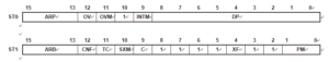
Below Figure shows the organization of status registers ST0 and ST1, indicating all status bits contained in each. Several bits in the status registers are reserved and are read as logic 1s to Break IC. Table 11 lists status register field definitions.