Dump NXP P89V52X2 Embedded Firmware
Hack will figure out the way to reset the watchdog to disable the security system and dump NXP P89V52X2 Embedded Firmware, Like a brown-out detect reset, the watchdog timer reset will clear the BSEL bit (FCF.0) but will not change the SWR bit (FCF.1) and therefore will not change the banking of the lower 8 kB of user code memory space.
The state of the SWR and BSEL bits after different types of resets is shown in below Table. This results in the code memory bank selections as shown.
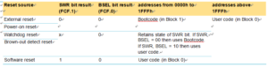
watchdog reset
The data RAM has 1024 bytes of internal memory. The device can also address up to 64 kB for external data memory.
The P89V52X2 has 1 kB of RAM. See Figure 6 “Internal and external data memory structure.” on page 19.
The device has four sections of internal data memory:
1. The lower 128 bytes of RAM (00H to 7FH) are directly and indirectly addressable.
2. The higher 128 bytes of RAM (80H to FFH) are indirectly addressable.
3. The special function registers (80H to FFH) are directly addressable only.
4. The expanded RAM of 768 bytes (00H to 2FFH) is indirectly addressable by the move external instruction (MOVX) and clearing the EXTRAM bit through MCU copying. (See ‘Auxiliary Register (AUXR) in Section 6 “Special function registers” on page 10).
Dump NXP P89V52X2 Embedded Firmware
Since the upper 128 bytes occupy the same addresses as the SFRs, the RAM must be accessed indirectly. The RAM and SFRs space are physically separate even though they have the same addresses.