-
Product Categories
-
Live Support Chat


Break MCU Chip Microchip PIC16F876A
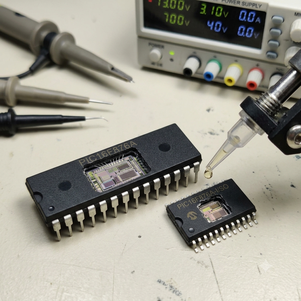
The Microchip PIC16F876A is an established 8-bit CMOS microcontroller featuring an enhanced mid-range RISC CPU core, a compact 28-pin footprint, integrated analog-to-digital converters, multi-channel PWM modules, and versatile serial communication protocols. Widely deployed in industrial motor controllers, automotive diagnostic nodes, medical instrumentation, and power management equipment, this versatile chip relies on integrated flash storage and internal eeprom arrays to run critical operational routines. To prevent commercial reverse-engineering and safeguard proprietary firmware logic, hardware developers regularly activate the device’s native code security configuration bits during manufacturing. This act of hardware protectionism locks the internal execution registers, creating a protective barrier across the physical silicon substrate that prevents standard debuggers, programming units, and logic analyzers from conducting an unauthorized readout of the embedded software.
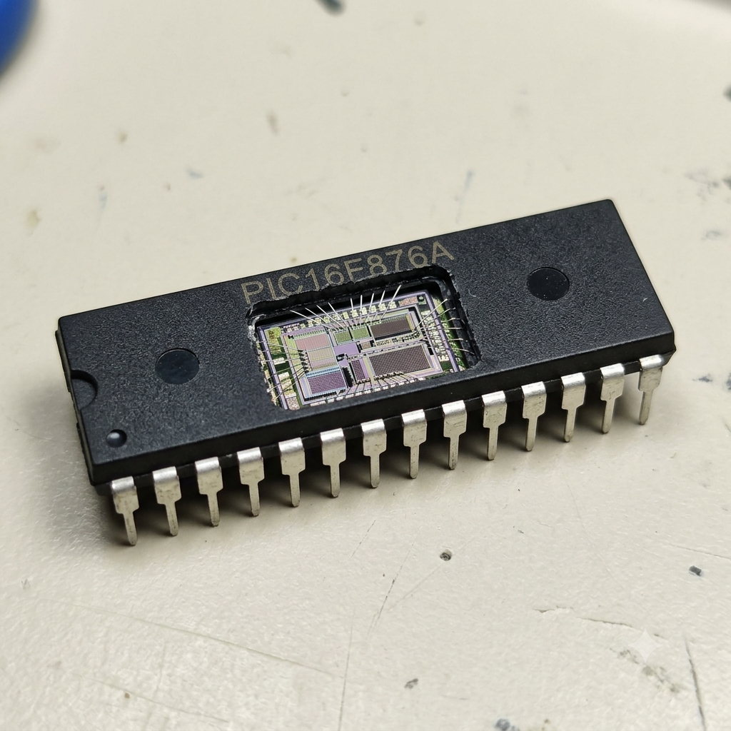
High-Performance RISC CPU:
· Only 35 single-word instructions to learn
· All single-cycle instructions except for program branches, which are two-cycle
· Operating speed: DC – 20 MHz clock input DC – 200 ns instruction cycle
· Up to 8K x 14 words of Flash Program Memory, Up to 368 x 8 bytes of Data Memory (RAM), Up to 256 x 8 bytes of EEPROM Data Memory
· Pinout compatible to other 28-pin or 40/44-pin PIC16CXXX and PIC16FXXX microcontrollers
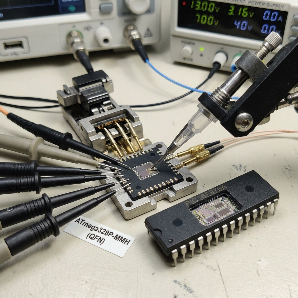
When a specialized engineering laboratory receives a mandate to break mcu chip microchip PIC16F876A security configurations or execute a clean readout from a protected system, the workflow moves into high-precision semiconductor engineering. To unlock, decrypt, or crack an encrypted microcontroller and execute a full data dump, technicians perform non-destructive physical circuit analysis directly on the chip substrate. Specialized microelectronics procedures—such as controlled voltage-glitching, thermal optimization, or focused micro-probing—are applied to temporarily disable the internal protective flags without corrupting the underlying gate logic. Once these hardware security barriers are temporarily bypassed, engineers can interface directly with the internal storage compartments, enabling them to copy, dump, and extract the embedded machine code into an uncorrupted binary or heximal file format for comprehensive system verification.
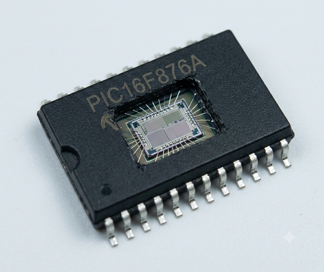
Peripheral Features:
· Timer0: 8-bit timer/counter with 8-bit prescaler
· Timer1: 16-bit timer/counter with prescaler, can be incremented during Sleep via external crystal/clock
· Timer2: 8-bit timer/counter with 8-bit period register, prescaler and postscaler
· Two Capture, Compare, PWM modules
– Capture is 16-bit, max. resolution is 12.5 ns
– Compare is 16-bit, max. resolution is 200 ns
– PWM max. resolution is 10-bit
· Synchronous Serial Port (SSP) with SPI™ (Master mode) and I2C™ (Master/Slave)
· Universal Synchronous Asynchronous Receiver Transmitter (USART/SCI) with 9-bit address detection
· Parallel Slave Port (PSP) – 8 bits wide with external RD, WR and CS controls (40/44-pin only)
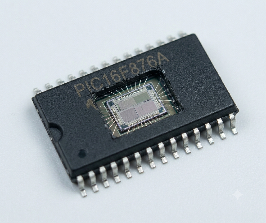
· Brown-out detection circuitry for Brown-out Reset (BOR)
The commercial imperative to replicate, copy, or fully extract legacy embedded code from an obsolete or completely outdate microchip framework is driven by modern supply chain realities and long-term asset preservation. Thousands of heavy manufacturing lines, utility sub-stations, and medical diagnostic facilities operate continuously under the control of legacy processing hardware that is no longer manufactured or supported by the original supplier. When the foundational source code repository is permanently lost due to historical drive failures, or the original design firm dissolves, a single controller breakdown can freeze a multi-million-dollar production line indefinitely. Extracting the compiled execution program directly from a functional backup module represents the only realistic method to maintain operational continuity. Reclaiming this vital operational data into an archival file allows corporate engineering teams to clone essential logic modules, replace damaged circuit boards, and preserve critical infrastructure without spending years of labor and millions of dollars rebuilding legacy software from scratch.

Analog Comparator module with:
– Two analog comparators
– Programmable on-chip voltage reference (VREF) module
– Programmable input multiplexing from device inputs and internal voltage reference
– Comparator outputs are externally accessible
Special Microcontroller Features:
· 100,000 erase/write cycle Enhanced Flash program memory typical
· 1,000,000 erase/write cycle Data EEPROM memory typical
· Data EEPROM Retention > 40 years
· Self-reprogrammable under software control
· In-Circuit Serial Programming™ (ICSP™) via two pins
· Single-supply 5V In-Circuit Serial Programming
· Watchdog Timer (WDT) with its own on-chip RC oscillator for reliable operation
· Programmable code protection
· Power saving Sleep mode
· Selectable oscillator options
· In-Circuit Debug (ICD) via two pins
CMOS Technology:
· Low-power, high-speed Flash/EEPROM technology
· Fully static design
· Wide operating voltage range (2.0V to 5.5V)
· Commercial and Industrial temperature ranges
· Low-power consumption
Our precision microelectronics facility delivers elite hardware analysis, logic bypass workflows, and seamless code recovery solutions for corporate end-users facing critical software preservation challenges. Our specialized engineering staff maintains extensive technical experience navigating complex multi-layer chip layouts across a broad catalog of hardware platforms, including specialized microcontrollers, complex programmable logic devices (cpld), arm processors, digital signal processors (dsp), and high-density altera chip architectures. Operating cleanroom-grade diagnostic platforms, we systematically work through localized hardware locks to retrieve hidden logic parameters while preserving the complete operational integrity of your master processing device. We transform raw hardware extractions into fully validated, production-ready firmware packages that can be directly written onto fresh replacement target components. Partnering with our specialized laboratory enables your business to eliminate costly redevelopment cycles, instantly recover lost build histories, and secure your long-term legacy investments. Contact our technical team today to arrange a precise evaluation for your chip recovery project.