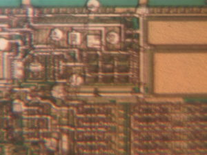
Crack Chip PIC18F4321 Eeprom
Crack Chip PIC18F4321 and disable the tamper resistance system of the memory, readout the data from MCU Eeprom and program from flash, duplicate the heximal into other blank Microcontroller PIC18F4321;

Crack Chip PIC18F4321 and disable the tamper resistance system of the memory, readout the data from Eeprom and program from flash, duplicate the heximal into other blank Microcontroller PIC18F4321
Devices in the PIC18F4321 family are available in 28-pin and 40/44-pin packages. Block diagrams for the two groups are shown in Figure 1-1 and Figure 1-2.
The devices are differentiated from each other in five ways:
Flash program memory (4 Kbytes for PIC18F2221/4221 devices, 8 Kbytes for PIC18F2321/4321).
A/D channels (10 for 28-pin devices, 13 for 40/44-pin devices).
I/O ports (3 bidirectional ports on 28-pin devices, 5 bidirectional ports on 40/44-pin devices). CCP and Enhanced CCP implementation (28-pin devices have 2 standard CCP modules, 40/44-pin devices have one standard CCP module and one ECCP module).
5. Parallel Slave Port (present only on 40/44-pin devices). All other features for devices in this family are identical. These are summarized in Table 1-1.
Like all Microchip PIC18 devices, members of the PIC18F4321 family are available as both standard and low-voltage devices. Standard devices with Enhanced Flash memory, designated with an “F” in the part number (such as PIC18F2321), accommodate an operating VDD range of 4.2V to 5.5V before Crack microcontroller pic16f506.
Low-voltage parts, designated by “LF” (such as PIC18LF2321), function over an extended VDD range of 2.0V to 5.5V. For timing insensitive applications, the RC and RCIO Oscillator modes offer additional cost savings. The actual oscillator frequency is a function of several factors:
· supply voltage
· values of the external resistor (REXT) and capacitor (CEXT)
· operating temperature
Given the same device, operating voltage, temperature and component values, there will also be unit-to-unit frequency variations. These are due to factors such as:
· normal manufacturing variation
· difference in lead frame capacitance between package types (especially for low CEXT values)
· variations within the tolerance of limits of REXT and CEXT
In the RC Oscillator mode, the oscillator frequency divided by 4 is available on the OSC2 pin. This signal may be used for test purposes or to synchronize other logic. Figure 2-5 shows how the R/C combination is connected after unlock microcontroller pic16f627a bin.
A Phase Locked Loop (PLL) circuit is provided as an option for users who wish to use a lower frequency oscillator circuit or to clock the device up to its highest rated frequency from a crystal oscillator.
This may be useful for customers who are concerned with EMI due to high-frequency crystals or users who require higher clock speeds from an internal oscillator.
The HSPLL mode makes use of the HS mode oscillator for frequencies up to 10 MHz. A PLL then multiplies the oscillator output frequency by 4 to produce an internal clock frequency up to 40 MHz. The PLLEN bit is not available when this mode is configured as the primary clock source.
The PLL is only available to the crystal oscillator when the FOSC3:FOSC0 Configuration bits are programmed for HSPLL mode (= 0110).
Tags: lesen chip dump,lesen ic program,lesen integrierte Schaltung eeprom,lesen mcu archive,lesen mikrocontroller flash

