What is PCB Reverse Engineering
PCB reverse engineering (PCB RE) refers to the process of analyzing and recreating the design drawing and functionality of a printed circuit board (PCB) without access to its original PCB board design files or documentation including Schematic diagram, Gerber file, Layout drawing and BOM list. It involves extracting information about the PCB’s components, circuit connections, and layout, usually through physical inspection, measurements, and testing.
The purpose of PCB reverse engineering can vary, but common reasons include:
- Replicating obsolete or outdated PCBs: When the original PCB design files or documentation are unavailable or lost, reverse engineering can help recreate the board to continue production or repair.
- Understanding competitor products: Reverse engineering PCB board allows companies to understand the design and technology used in competitor PCBs, which can be useful for product benchmarking or feature comparison.
- Identifying security vulnerabilities: Reverse engineering printed circuit board can help identify potential security flaws or vulnerabilities in PCB designs, allowing for improvements or countermeasures to be implemented.
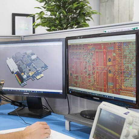
The reverse engineering PCB board process typically involves physical assessment and measurement of the PCB, such as tracing connections using multimeters, identifying components and their values, and examining the PCB layout. Advanced techniques like X-ray imaging or scanning electron microscopy may also be used to analyze the internal structures of integrated circuits.
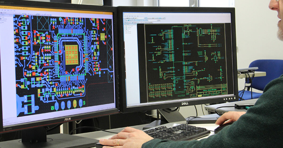
Once the necessary information is gathered, it can be used to recreate the PCB design. This may involve creating a new schematic diagram or PCB layout in design software, selecting the appropriate components, and then manufacturing the PCB using the recreated design.