PCB Board Reverse Engineering Process
First step of PCB Board Reverse Engineering, it is to record of all the components’ designators, locations, specification and part number, especially the orientation of diode, triode and integrated circuits. Better use camera to take some photos of these parts;
Secondly, de-solder all of the components, and remove all of the tin residual in the PAD vias or holes, use alcohol to wipe out the dirt and residue on the PCB Board, put it into scanning device, active PHOTOSHOP, then scan the image of silkscreen layer by using colorful scanning and print it out;
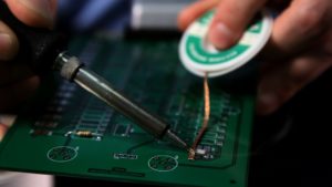
desolder component off PCB board
Third, use sandpaper to scrub TOP & BOTTOM Layer gently till the copper area is fully exposed, put it into the scanning device and active the PHOTOSHOP software, scanning them all by colorful mode. The orientation of PCB Board placing in the scanning device must be 90 degree upright and horizontal to the edge of frame of scanning device otherwise the image won’t be able to use in the subsequent reverse engineering process;
The forth step is adjust the scanning pictures with contrast and shading, to ensure the part with copper circuitry pattern and the area without the copper circuitry pattern has sharp contrast then convert the secondary pictures into BLACK/WHITE version, check if the line and tracks on the PCB Board is clear or not, if it is not clear need to repeat this step. If the result is ok, then save the image as BLACK/WHITE BMP format and name as TOP & BOT;
Fifth, input these two BMP files into PROTEL files, and introduce two layers from PROTEL which the most commonly used software for PCB Board Reverse Engineering, if the Pads and Vias on these two layers can overlap with each other perfectly, means the work which have been done from previous steps are well, otherwise designer has to repeat the steps of number third;
Sixth, convert the TOP.BMP into TOP.PCB, and engineer need to convert it to SILK layer and then draw the layout diagram on the TOP layer, and place the components according to the record acquired from step 2, after the layout diagram has been completed the SILK layer has to be deleted.
Seventh, convert the BOT.BMP layer into BOT.PCB, same as previous step;
Eighth, introduce TOP.PCB & BOT.PCB in the PROTEL software and integrate into one image;
Ninth, use laser printer to print TOP LAYER, BOT LAYER onto the transparent film as 1:1 ratio, and place the film onto the PCB image for comparison, if they can match 100% means the success of PCB Board Reverse Engineering;