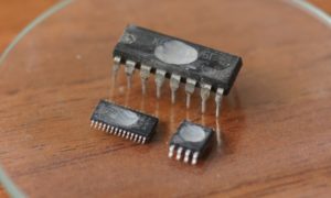
Unlock PIC16LF689 MCU Memory Source Code
Unlock PIC16LF689 MCU memory source code starts from crack PIC16LF689 secured microcontroller fuse bit, dump embedded firmware in the format of binary data or heximal file to new PIC16LF689 microprocessor;
To read a program memory location when Unlock PIC16LF689 MCU Memory Source Code, the user must write two bytes of the address to the EEADR and EEADRH registers, set the EEPGD control bit (EECON1<7>) and then set control bit, RD (EECON1<0>). Once the read control bit is set, the program memory Flash controller will use the second instruction cycle to read the data after Crack MCU ST7FLITEBCM6 Locked Eeprom.
This causes the second instruction immediately following the “BSF EECON1, RD” instruction to be ignored to Break IC. The data is available in the very next cycle in the EEDATA and EEDATH registers; therefore, it can be read as two bytes in the following instructions.
EEDATA and EEDATH registers will hold this value until another read or until it is written to by the user (during a write operation). The minimum erase block is 32 words. Only through the use of an external programmer, or through ICSP control, can larger blocks of program memory be bulk erased in the process of MCU PIC16LF648A Flash Program Decoding.
Word erase in the Flash array is not supported. When initiating an erase sequence from the micro- controller itself, a block of 32 words of program memory is erased. The Most Significant 11 bits of the EEADRH:EEADR point to the block being erased. EEADR< 4:0> are ignored.
The EECON1 register commands the erase operation. The EEPGD bit must be set to point to the Flash program memory which can be obtained from Replicate S3F84U8 Microcontroller Flash Heximal. The WREN bit must be set to enable write operations which will facilitate the process of Unlock PIC16LF689 MCU Memory Source Code. The FREE bit is set to select an erase operation. For protection, the write initiate sequence for EECON2 must be used.
After the “BSF EECON1, WR” instruction, the processor requires two cycles to set up the erase operation. The user must place two NOP instructions after the WR bit is set to provide the support from Unlock MC68HC08GP32 Chip Flash. The processor will halt internal operations for the typical 2 ms, only during the cycle in which the erase takes place.