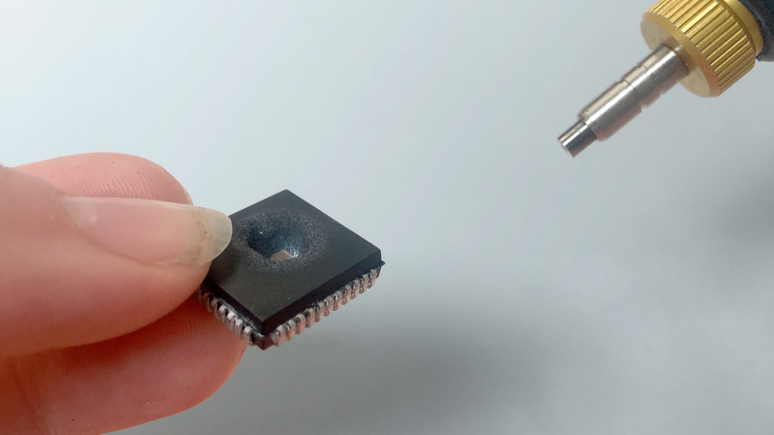
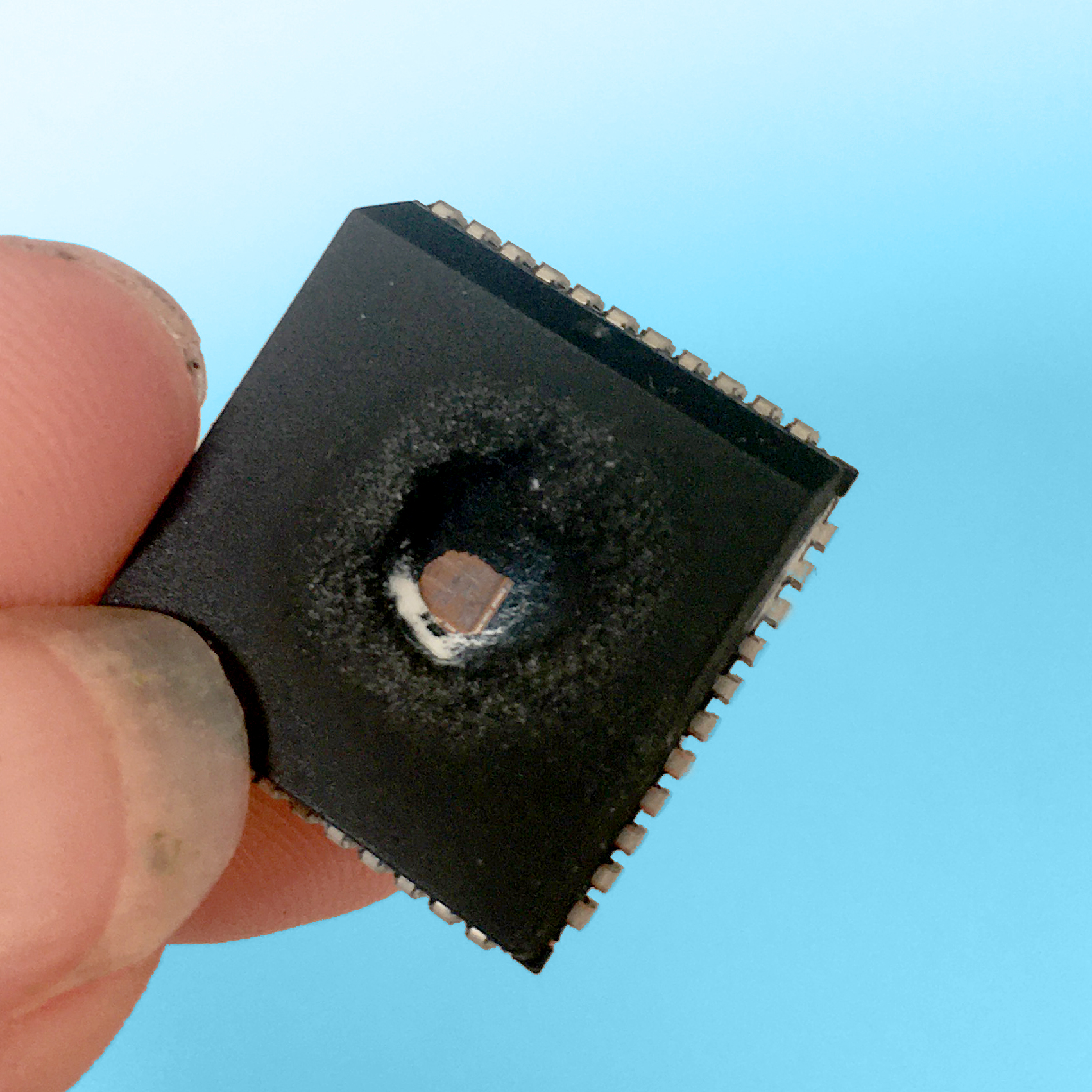
Unlock DSP Microprocessor TMS320F28375 Flash Memory
Unlock DSP Microprocessor TMS320F28375 Flash Memory and eeprom memory, the embedded firmware of mcu tms320f28375 will be decrypted and copy binary to new microcontroller;
Below Figure shows the connection between the MCU and JTAG header for a single-processor configuration. If the distance between the JTAG header and the MCU is greater than 6 inches, the emulation signals must be buffered.
If the distance is less than 6 inches, buffering is typically not needed. Below Figure shows the simpler, no-buffering situation. For the pullup and pulldown resistor values when cracking dsp microcontroller tms320f28051 flash memory.
The 283xx devices do not have EMU0/EMU1 pins. For designs that have a JTAG Header onboard, the EMU0/EMU1 pins on the header must be tied to VDDIO through a 4.7-kΩ (typical) resistor.
Qualifier
- This glitch will be ignored by the input qualifier. The QUALPRD bit field specifies the qualification sampling period. The QUALPRD bit field value can vary from 00 to 0xFF. If QUALPRD = 00, then the sampling period is one SYSCLKOUT cycle. For any other value “n”, the qualification sampling period in 2n SYSCLKOUT cycles (that is, at every 2n SYSCLKOUT cycles, the GPIO pin will be sampled).
- The qualification period selected through the GPxCTRL register applies to groups of eight GPIO pins.
- The qualification block can take either three or six samples. The GPxQSELn Register selects which sample mode is used.
- In the example shown, for the qualifier to detect the change, the input should be stable for 10 SYSCLKOUT cycles or greater. In other words, the inputs should be stable for (5 × QUALPRD × 2) SYSCLKOUT cycles. This would ensure five sampling periods for detection to occur. Because external signals are driven asynchronously, an 13- SYSCLKOUT-wide pulse ensures reliable recognition.