Read IC PIC16F88 Data
Read IC PIC16F88 Data out from its eeprom and program from flash memory, the process will start from decapsulate the microcontroller silicon package and get access to the security fuse bit then cut it off by Microprocessor breaking;
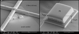
Read IC PIC16F88 Data out from its eeprom and program from flash memory, the process will start from decapsulate the microcontroller silicon package and get access to the security fuse bit then cut it off by Microprocessor breaking
This document contains device specific information for the operation of the PIC16F87/88 devices. Additional information may be found in the PICmicro® Mid-Range MCU Reference Manual (DS33023) which may be downloaded from the Microchip web site. This Reference Manual should be considered a complementary document to this data sheet, and is highly recommended reading for a better understanding of the device architecture and operation of the peripheral modules after Microcontroller atmega162 firmware discovery.
The PIC16F87/88 belongs to the Mid-Range family of the PICmicro® devices. Block diagrams of the devices are shown in Figure 1-1 and Figure 1-2. These devices contain features that are new to the PIC16 product line:
· Low-power modes: RC_RUN allows the core and peripherals to be clocked from the INTRC, while SEC_RUN allows the core and peripherals to be clocked from the low-power Timer1. Refer to Section 4.7 “Power Managed Modes” for further details for CPLD Altera EPM7064LC44 reverse engineering.
· Internal RC oscillator with eight selectable frequencies, including 31.25 kHz, 125 kHz, 250 kHz, 500 kHz, 1 MHz, 2 MHz, 4 MHz, and 8 MHz. The INTRC can be configured as a primary or secondary clock source. Refer to Section 4.5 “Internal Oscillator Block” for further details after Renesas MCU R5F21388CNFP reverse engineering.
· The Timer1 module current consumption has been greatly reduced from 20 µA (previous PIC16 devices) to 1.8 µA typical (32 kHz at 2V), which is ideal for real-time clock applications. Refer to Section 7.0 “Timer1 Module” for further details.
· Extended Watchdog Timer (WDT) that can have a programmable period from 1 ms to 268s. The WDT has its own 16-bit prescaler. Refer to further details.
· Two-Speed Start-up: When the oscillator is configured for LP, XT, or HS, this feature will clock the device from the INTRC while the oscillator is warming up. This, in turn, will enable almost immediate code execution;
· Fail-Safe Clock Monitor: This feature will allow the device to continue operation if the primary or secondary clock source fails by switching over to the INTRC.
· The A/D module has a new register for PIC16 devices named ANSEL. This register allows easier configuration of analog or digital I/O pins.
Tags: read ic heximal archive,read ic heximal code,read ic heximal content,read ic heximal data,read ic heximal eeprom,read ic heximal file,read ic heximal firmware,read ic heximal information,read ic heximal memory,read ic heximal program