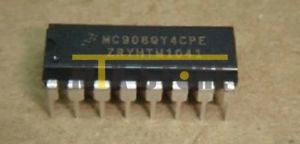
MC68HC908QY4 CPU Embedded Firmware Cloning
FLASH Page Erase Operation can be taken out when carry on the MC68HC908QY4 CPU Embedded Firmware Cloning:
Use this step-by-step procedure to erase a page (128 bytes) of FLASH memory to read as logic 1:
- Set the ERASE bit, and clear the MASS bit in the FLASH control register.
- Read the FLASH block protect register.
- Write any data to any FLASH address within the page address range desired.
- Wait for a time, tnvs (min. 10ms)
- Set the HVEN bit.
- Wait for a time, tErase (min. 1ms)
- Clear the ERASE bit.
- Wait for a time, tnvh (min. 5ms)Use this step-by-step procedure to erase a page (128 bytes) of FLASH memory to read as logic 1:
1. Set the ERASE bit, and clear the MASS bit in the FLASH control register.
2. Read the FLASH block protect register.
3. Write any data to any FLASH address within the page address range desired.
4. Wait for a time, tnvs (min. 10s)
5. Set the HVEN bit.
6. Wait for a time, tErase (min. 1ms)
7. Clear the ERASE bit.
8. Wait for a time, tnvh (min. 5s)
Clear the HVEN bit.
MC68HC908QY4 CPU Embedded Firmware Cloning
After a time, trcv (typ. 1ms), the memory can be accessed again in read mode.
While these operations must be performed in the order shown, other unrelated operations may occur between the steps in the process of Break MC68HC908EY16 Microprocessor Protected Flash.
Use this step-by-step procedure to erase entire FLASH memory to read as logic 1:
- Set both the ERASE bit, and the MASS bit in the FLASH control register.
- Read from the FLASH block protect register.
- Write any data to any FLASH address* within the FLASH memory address range.
- Wait for a time, tnvs (min. 10ms)
- Set the HVEN bit.
- Wait for a time, tMErase (min. 4ms)
- Clear the ERASE bit.
- Wait for a time, tnvhl (min. 100ms)
- Clear the HVEN bit.
- After a time, trcv (min. 1ms), the memory can be accessed again in read mode.
* When in Monitor mode, with security sequence failed, write to the FLASH block protect register instead of any FLASH address on the MC68HC908QY4 CPU Embedded Firmware Cloning.
NOTE: Programming and erasing of FLASH locations cannot be performed by code being executed from the FLASH memory. While these operations must be performed in the order shown, other unrelated operations may occur between the steps.