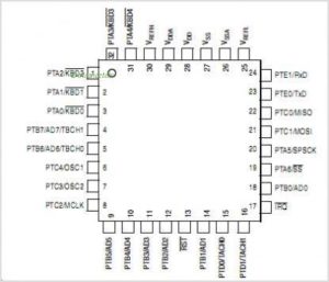
Break MC68HC908EY16 Microprocessor Protected Flash
FLASH Program/Read Operation is very critical features for Break MC68HC908EY16 Microprocessor Protected Flash, below we will introduce its basic features:
Programming of the FLASH memory is done on a row basis. A row consists of 64 consecutive bytes starting from addresses $XX00,
$XX40, $0080 and $XXC0. Use this step-by-step procedure to program a row of FLASH memory when Reading MCU (Figure 4-2 is a flowchart representation):
NOTE: In order to avoid program disturbs, the row must be erased before any byte on that row is programmed.
- Set the PGM bit. This configures the memory for program operation and enables the latching of address and data for programming.
- Read from the FLASH block protect register.
- Write any data to any FLASH address within the row address range desired.
- Wait for a time, tnvs (min. 10ms).
- Set the HVEN bit.
- Wait for a time, tpgs (min. 5ms).
- Write data to the FLASH address to be programmed.*
- Wait for a time, tPROG (min. 30ms).
- Repeat step 7 and 8 until all the bytes within the row are programmed.
- Clear the PGM bit.*
- Wait for a time, tnvh (min. 5ms).
- Clear the HVEN bit.
- After time, trcv (min. 1ms), the memory can be accessed in read mode again.
The time between each FLASH address change, or the time between the last FLASH address programmed to clearing PGM bit, must not exceed the maximum programming time, tPROG max after Break MC68HC908EY16 Microprocessor Protected Flash.
This program sequence is repeated throughout the memory until all data is programmed.


