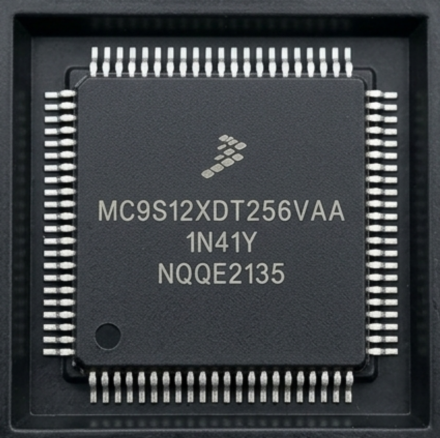
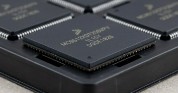
Decrypt Microprocessor IC Freescale MC9S12XDT256
The Freescale MC9S12XDT256 represents a powerful evolution in the 16-bit MCU landscape, widely utilized in high-performance automotive electronics, industrial automation, and complex engine control units. This Microchip is engineered with a massive 256KB of FLASH MEMORY, alongside EEPROM and high-speed RAM, allowing it to handle sophisticated multitasking environments. Because of its critical role in proprietary vehicle systems and industrial logic, the IC is equipped with advanced PROTECTIVE measures. These security protocols are designed to ensure the internal FIRMWARE remains LOCKED and inaccessible to unauthorized parties. This level of digital protectionism is vital for manufacturers to guard their SOURCE CODE, but it presents a significant challenge when the hardware becomes OBSOLETE and maintenance requires access to the original DATA.
To Decrypt Microprocessor IC Freescale MC9S12XDT256 units, engineers must engage in a meticulous process known as a security UNLOCK. This procedure is specifically designed to bypass the ENCRYPTED lock bits that prevent a standard READOUT of the BINARY or HEXIMAL code. When a Chip is LOCKED, the traditional debugging interfaces are restricted, making it impossible to COPY or REPLICATE the internal PROGRAM through conventional means. By utilizing specialized laboratory equipment, experts can CRACK the security barrier, allowing them to DUMP the full contents of the FLASH and EEPROM. This technical DECRYPT operation ensures that the core SOFTWARE can be extracted and preserved as a high-integrity FILE, facilitating a perfect REPLICATE of the device’s original functionality for backup or migration purposes.
Targeted at automotive multiplexing applications, the MC9S12XD Family will deliver 32-bit performance with all the advantages and efficiencies of a 16-bit MCU. The S12X is designed to retain the low cost, low power consumption, excellent EMC performance and code-size efficiency advantages enjoyed by users of Freescale’s previous 16-bit MC9S12 MCU family. Based around an enhanced S12 core, the MC9S12XD Family will deliver two to five times the performance of a 25 MHz S12 whilst retaining a high degree of pin and code compatibility with the original S12D – family.
The MC9S12XD Family features the performance boosting XGATE co-processor. The XGATE, which is programmable in “C” language, has an instruction set which is optimized for data movement, logic and bit manipulation instructions. It runs at twice the bus frequency of the S12X and off-loads the CPU by providing high speed data transfer (and data processing) between any peripheral module, RAM and I/O ports. This is particularly useful in applications such as automotive gateways where there are multiple busses carrying heavy data traffic which would otherwise exert a heavy interrupt/processing load on the CPU. The MC9S12XD Family will feature an enhanced MSCAN module which, when used in conjunction with XGATE, delivers FullCAN performance with virtually unlimited number of mailboxes and retains backwards compatibility with the MSCAN module featured on previous S12 products.
Memory options will range from 64 Kbytes to 512 Kbytes of Freescale’s industry-leading, full automotive spec SG-Flash with additional integrated EEPROM. In addition to the rich S12 peripheral set, the MC9S12XD Family will feature more RAM, extra A/D channels, new timer features and additional LIN-compatible SCI ports compared with the original S12 D-Family. The MC9S12XD Family also features a new flexible interrupt handler which allows multilevel nested interrupts. The MC9S12XD Family has full 16-bit data paths throughout. The non-multiplexed expanded bus interface available on the 144-pin versions allows an easy interface to external memories.
The inclusion of a PLL circuit allows power consumption and performance to be adjusted to suit operational requirements. System power consumption is further improved with the new “fast exit from STOP mode” feature and an ultra low power wakeup timer. In addition to the I/O ports available in each module, up to 25 further I/O ports are available with interrupt capability allowing wakeup from STOP or WAIT mode. The MC9S12XD Family will be available in 144-pin LQFP (with optional external bus), 112-pin, and 80-pin options.
The global demand to DUMP and REPLICATE the FIRMWARE from an ENCRYPTED Microprocessor is driven by the necessity of industrial longevity. Many sectors rely on OUTDATE machinery where the MC9S12XDT256 is the central brain; if the original manufacturer no longer provides support or the SOURCE CODE has been lost, the entire system is at risk of becoming OBSOLETE. There is an essential market need to UNLOCK and READOUT these components to prevent catastrophic downtime. Whether it is a legacy ARM, DSP, or CPLD controller, the ability to COPY and DECRYPT the DATA is the only way to ensure that critical infrastructure can be repaired or cloned when official replacement parts are no longer available in the supply chain.
Our facility provides a world-class service to Decrypt Microprocessor IC Freescale MC9S12XDT256 for clients requiring deep-level hardware recovery. We possess the technical mastery to UNLOCK, CRACK, and READOUT highly PROTECTIVE Microchip architectures, delivering a flawless HEXIMAL or BINARY FILE for your engineering team. Our capabilities extend across a vast array of IC types, ensuring that your ENCRYPTED SOURCE CODE and FIRMWARE are retrieved with 100% accuracy. By offering a secure way to REPLICATE and DUMP the DATA from OUTDATE or LOCKED units, we help you overcome the hurdles of component obsolescence. Trust our experts to handle your most sensitive MEMORY extraction needs, providing the vital SOFTWARE continuity required to keep your operations running smoothly.