Break NXP MC908SR12 Microcontroller Flash
The FLASH block protect register (FLBPR) is implemented as a byte within the FLASH memory which is quite useful for Break NXP MC908SR12 Microcontroller Flash, and therefore can only be written during a programming sequence of the FLASH memory. The value in this register determines the starting location of the protected range within the FLASH memory.
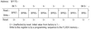
FLASH Block Protect Register (FLBPR)
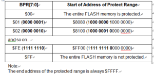
These eight bits represent bits [14:7] of a 16-bit memory address. Bit-15 is logic 1 and bits [6:0] are logic 0s. The resultant 16-bit address is used for specifying the start address of the FLASH memory for block protection.
The FLASH is protected from this start address to the end of FLASH memory, at $FFFF. With this mechanism, the protect start address can be XX00 and XX80 (128 bytes page boundaries) within the FLASH memory.
Putting the MCU into wait mode while the FLASH is in read mode does not affect the operation of the FLASH memory directly, but there will not be any memory activity since the CPU is inactive after Break MC68HC908EY16 Microprocessor Protected Flash.
The WAIT instruction should not be executed while performing a program or erase operation on the FLASH, otherwise the operation will discontinue, and the FLASH will be on Standby Mode.
Putting the MCU into stop mode while the FLASH is in read mode does not affect the operation of the FLASH memory directly, but there will not be any memory activity since the CPU is inactive.
The STOP instruction should not be executed while performing a program or erase operation on the FLASH, otherwise the operation will discontinue, and the FLASH will be on Standby Mode after MCU Reading.
Standby Mode is the power saving mode of the FLASH module in which all internal control signals to the FLASH are inactive and the current consumption of the FLASH is at a minimum.