-
Product Categories
Live Support Chat


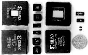
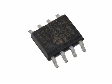
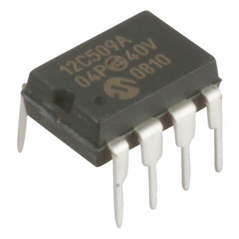
Read Microcontroller PIC12C509A Binary
Read Microcontroller PIC12C509A Binary from embedded memory, copy the firmware of mcu pic12c509a out, in order to completely extracted code from mcu pic12c509a flash and eeprom memory, we have to crack the MCU firstly;
PIC12C5XX memory is organized into program memory and data memory. For devices with more than 512 bytes of program memory, a paging scheme is used if Read Microcontroller.
Program memory pages are accessed using one STATUS register bit. For the PIC12C509, PIC12C509A, PICCR509A and PIC12CE519 with a data memory register file of more than 32 registers, a banking scheme is used. Data memory banks are accessed using the File Select Register (FSR) when Read Microcontroller.
The PIC12C5XX devices have a 12-bit Program Counter (PC) capable of addressing a 2K x 12 program memory space. Only the first 512 x 12 (0000h-01FFh) for the PIC12C508, PIC12C508A and PIC12CE518 and 1K x 12 (0000h-03FFh) for the PIC12C509, PIC12C509A, PIC12CR509A, and PIC12CE519 are physically implemented after Read Microcontroller. Refer to Figure 4-1. Accessing a location above these boundaries will cause a wrap around within the first 512 x 12 space (PIC12C508, PIC12C508A and PIC12CE518) or 1K x 12 space (PIC12C509, PIC12C509A, PIC12CR509A and PIC12CE519) if Read Microcontroller. The effective reset vector is at 000h, (see Figure 4-1). Location 01FFh (PIC12C508, PIC12C508A and PIC12CE518) or location 03FFh (PIC12C509, PIC12C509A, PIC12CR509A and PIC12CE519) contains the internal clock oscillator calibration value. This value should never be overwritten when Read Microcontroller.
As a program instruction is executed, the Program Counter (PC) will contain the address of the next program instruction to be executed. The PC value is increased by one every instruction cycle, unless an instruction changes the PC.
For a GOTO instruction, bits 8:0 of the PC are provided by the GOTO instruction word. The PC Latch (PCL) is mapped to PC<7:0>. Bit 5 of the STATUS register provides page information to bit 9 of the PC (Figure 4- 8).For a CALL instruction, or any instruction where the PCL is the destination before unlock Microcontroller chip, bits 7:0 of the PC again are provided by the instruction word. However, PC<8> does not come from the instruction word, but is always cleared.
Instructions where the PCL is the destination, or Modify PCL instructions, include MOVWF PC, ADDWF PC, and BSF PC,5. The Program Counter is set upon a RESET, which means that the PC addresses the last location in the last page i.e., the oscillator calibration instruction. After executing MOVLW XX, the PC will roll over to location 00h, and begin executing user code.
The STATUS register page preselect bits are cleared upon a RESET, which means that page 0 is pre-selected. Therefore, upon a RESET, a GOTO instruction will automatically cause the program to jump to page 0 until the value of the page bits is altered if unlocking Microcontroller.