-
Product Categories
Live Support Chat


Microchip PIC12LC508 CPU Memory Replication
Microchip PIC12LC508 CPU Memory Replication
PIC12LC508 cpu memory is organized into program memory and data memory. For the PIC12LC508, a paging scheme is used for the purpose of Recover MCU Firmware. Program memory pages are accessed using one STATUS register bit. Data memory banks are accessed using the File Select Register (FSR) to perform the Microchip PIC12LC508 CPU Memory Replication.
The PIC12LC508 devices have a 12-bit Program Counter (PC). The 1K x 12 (0000h-03FFh) for the PIC12LC508 are physically implemented when STM32F100ZC CPU Memory Cracking. Accessing a location above this boundary will cause a wrap-around within the first 1K x 12 space. The effective reset vector is at 0000h. Location 03FFh (PIC16C505) contains the internal clock oscillator calibration value. This value should never be overwritten.
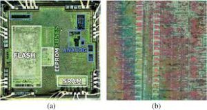
Microchip PIC12LC508 CPU Memory Replication
Data memory is composed of registers, or bytes of RAM from Microcomputer S3P9234 Memory Program Cloning. Therefore, data memory for a device is specified by its register file. The register file is divided into two functional groups: special function registers and general purpose registers.
The special function registers include the TMR0 register, the Program Counter (PC), the Status Register, the I/O registers (ports), and the File Select Register (FSR) through Extract IC PIC16F884 Code. In addition, special purpose registers are used to control the I/O port configuration and prescaler options. The general purpose registers are used for data and control information under command of the instructions.
For the PIC12LC508, the register file is composed of 8 special function registers, 24 general purpose registers, and 48 general purpose registers that may be addressed using a banking scheme when Break DSP Controller TMS320F2806PZA Memory.