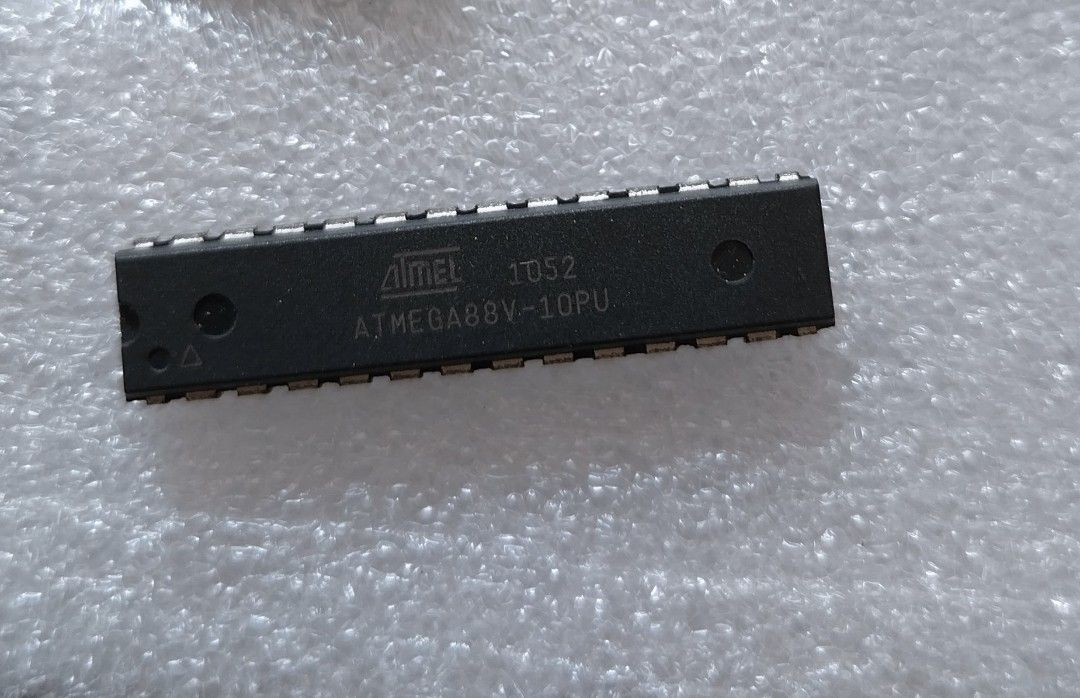
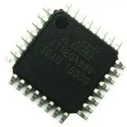
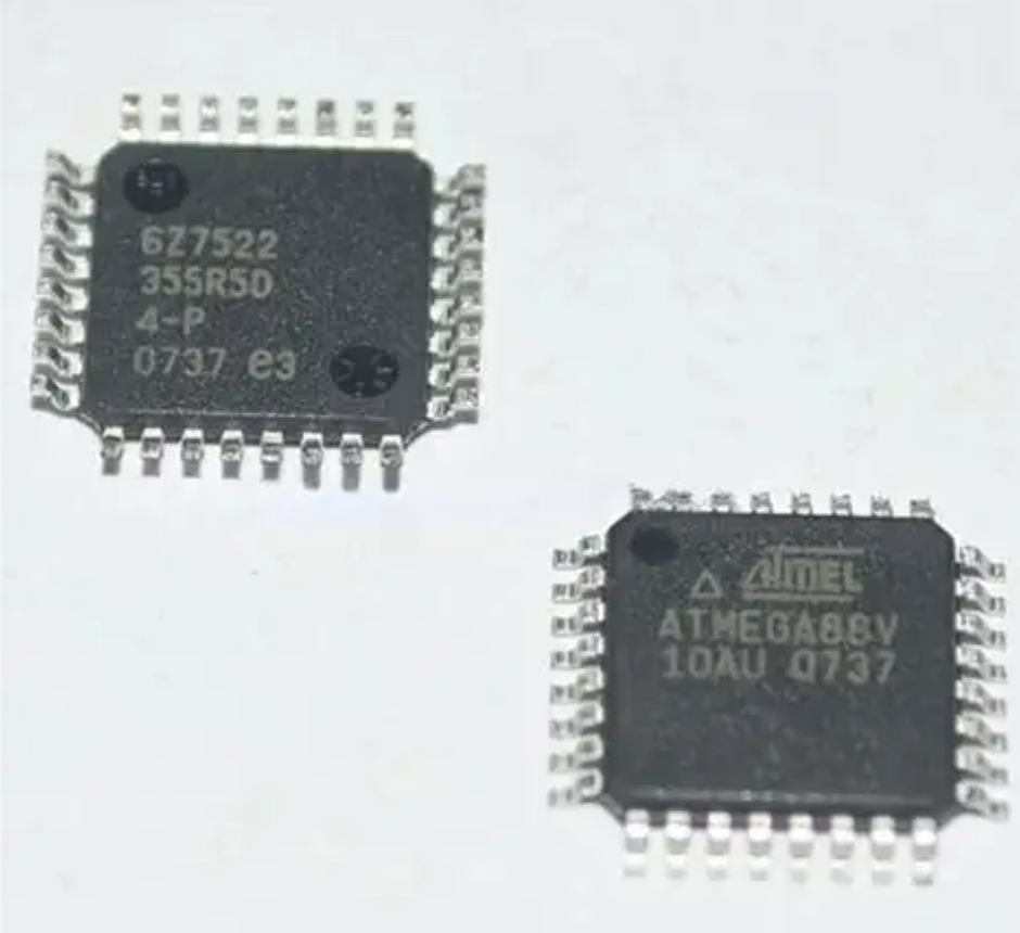
The Atmel ATmega88V is a low-voltage, high-efficiency microcontroller celebrated for its versatility in battery-powered applications and precision instrumentation. As a pivotal member of the AVR family, this MCU is extensively deployed in handheld consumer electronics, wireless sensor nodes, and smart metering systems. To defend the sensitive firmware contained within its FLASH and EEPROM memory, the chip utilizes a sophisticated protective architecture. By engaging internal “Lock Bits,” the microchip effectively becomes an encrypted vault. This hardware-level security is designed to ensure that the proprietary program and internal data are shielded from unauthorized readout, maintaining the integrity of the manufacturer’s intellectual property.
Когда профессиональной лаборатории поручают разблокировать защищённый микроконтроллер Atmel ATmega88V, это требует глубокого изучения логики кремния для обхода активных защитных барьеров. Для обнаружения внутренней структуры микроконтроллера AVR Atmel ATmega88V инженеры используют специализированное оборудование для расшифровки состояния предохранителя безопасности без повреждения микропроцессора Atmel ATmega88V. Этот процесс позволяет специалисту получить доступ к сохранённому двоичному или шестнадцатеричному файлу, обеспечивая чёткое представление об исходном наборе инструкций микропроцессора. Независимо от того, является ли целью взлом битов блокировки для криминалистического анализа или чтение прошивки для резервного копирования, эта процедура является основным методом извлечения исходного кода из заблокированного или зашифрованного микрочипа Atmel ATmega88V. Глобальный спрос на репликацию или копирование микроконтроллеров Atmel ATmega88V обусловлен реалиями промышленного жизненного цикла, когда оборудование часто устаревает или выходит из строя. Многие важные системы в производственном и энергетическом секторах используют устаревшие компоненты ARM, DSP или CPLD, которые больше не производятся. Когда критически важный микроконтроллер Atmel ATmega88V выходит из строя, а исходное программное обеспечение или код недоступны, возможность расшифровки и копирования существующей прошивки становится необходимостью, а не просто опцией.
When a professional laboratory is tasked to unlock a secured microcontroller, it involves a deep-dive into the silicon’s logic to bypass these active security barriers. To discover AVR MCU Atmel ATmega88V internal structures, engineers use specialized equipment to decrypt the security fuse state without damaging the IC. This process allows the technician to dump the stored binary or heximal file, providing a clear window into the microprocessor’s original instruction set. Whether the goal is to crack the lock bits for forensic analysis or to readout the firmware for backup, this procedure is the primary method for extracting source code from a locked or encryptedmicrochip.
Cuando un laboratorio profesional recibe el encargo de desbloquear un microcontrolador Atmel ATmega88V protegido, se requiere un análisis exhaustivo de la lógica del chip para sortear las barreras de seguridad activas. Para descubrir las estructuras internas del AVR MCU Atmel ATmega88V, los ingenieros utilizan equipos especializados para descifrar el estado del fusible de seguridad sin dañar el microprocesador. Este proceso permite al técnico extraer el archivo binario o hexadecimal almacenado, lo que proporciona una visión clara del conjunto de instrucciones original del microprocesador. Ya sea que el objetivo sea descifrar los bits de bloqueo para un análisis forense o leer el firmware para realizar copias de seguridad, este procedimiento es el método principal para extraer el código fuente de un microcontrolador Atmel ATmega88V bloqueado o cifrado. La demanda global de replicar o copiar un microcontrolador Atmel ATmega88V se debe a la realidad de los ciclos de vida industriales, donde el hardware a menudo se vuelve obsoleto. Muchos sistemas esenciales en los sectores de fabricación y energía dependen de componentes ARM, DSP o CPLD antiguos que ya no se fabrican. Cuando falla un microcontrolador Atmel ATmega88V crítico y el software o el código fuente original no están disponibles, la capacidad de descifrar y copiar el firmware existente se convierte en una necesidad más que en una opción.
The global demand to replicate or copy a microcontroller is driven by the reality of industrial lifecycles where hardware often becomes obsolete or outdate. Many essential systems in the manufacturing and energy sectors rely on older ARM, DSP, or CPLD components that are no longer in production. When a critical chip fails and the original software or source code is unavailable, the ability to decrypt and copy the existing firmware becomes a necessity rather than an option. This market need is vital for maintaining legacy infrastructure, ensuring that a single outdateIC doesn’t lead to the complete decommissioning of an expensive, otherwise functional machine.
Professional Recovery and Technical Expertise
Our facility provides industry-leading services to discover AVR MCU Atmel ATmega88V logic and provide comprehensive recovery solutions for end-users. We specialize in navigating the complexities of locked hardware to ensure your operations remain uninterrupted. Our core competencies include:
Security Bypass: We possess the technical mastery to unlock and decrypt a wide variety of protectiveMCU and CPLD devices.
Data Extraction: Our team can accurately dump and readout internal FLASH and EEPROM, delivering the resulting data as a stable binary or heximal file.
Legacy Support: We help clients replicate and copyobsolete components, providing a path forward when original manufacturers cease support for older microprocessor models.
Firmware Integrity: By retrieving the source code or firmware directly from the microchip, we help you recreate lost software assets for critical system repairs.
In an era where technology moves fast, staying tethered to outdate or obsolete hardware can be a liability. We provide the key to unlock those barriers, allowing you to replicate essential components and secure the firmware that drives your business. Our commitment is to provide a reliable, precise service that restores your access to the data trapped inside encrypted silicon, ensuring your legacy systems continue to perform at their peak.
Quando un laboratorio specializzato viene incaricato di sbloccare un microcontrollore Atmel ATmega88V protetto, ciò comporta un’analisi approfondita della logica del silicio per aggirare le barriere di sicurezza attive. Per scoprire le strutture interne di un microcontrollore AVR Atmel ATmega88V, gli ingegneri utilizzano apparecchiature specializzate per decifrare lo stato del fusibile di sicurezza senza danneggiare il microprocessore Atmel ATmega88V. Questo processo consente al tecnico di estrarre il file binario o esadecimale memorizzato, fornendo una chiara visione del set di istruzioni originale del microprocessore. Che l’obiettivo sia decifrare i bit di blocco per l’analisi forense o leggere il firmware per il backup, questa procedura è il metodo principale per estrarre il codice sorgente da un microcontrollore Atmel ATmega88V bloccato o crittografato. La domanda globale di replicare o copiare un microcontrollore Atmel ATmega88V è dettata dalla realtà dei cicli di vita industriali, in cui l’hardware diventa spesso obsoleto. Molti sistemi essenziali nei settori manifatturiero ed energetico si basano su componenti ARM, DSP o CPLD più vecchi che non sono più in produzione. Quando un microcontrollore Atmel ATmega88V critico si guasta e il software originale o il codice sorgente non sono disponibili, la capacità di decrittografare e copiare il firmware esistente diventa una necessità, non un’opzione.
Depending on the clock selection fuse settings, PB6 can be used as input to the inverting Oscillator amplifier and input to the internal clock operating circuit. Depending on the clock selection fuse settings, PB7 can be used as output from the inverting Oscillator amplifier.
If the Internal Calibrated RC Oscillator is used as chip clock source, PB7..6 is used as TOSC2..1 input for the Asynchronous Timer/Counter2 if the AS2 bit in ASSR is set when pull program from mcu.
The various special features of Port B are elaborated in “Alternate Functions of Port B” on page 69 and “System Clock and Clock Options” on page 24. Port C is a 7-bit bi-directional I/O port with internal pull-up resistors (selected for each bit).
The PC5..0 output buffers have symmetrical drive characteristics with both high sink and source capability. As inputs, Port C pins that are externally pulled low will source current if the pull-up resistors are activated.
The Port C pins are tri-stated when a reset condition becomes active, even if the clock is not running. If the RSTDISBL Fuse is programmed, PC6 is used as an I/O pin.
If the RSTDISBL Fuse is unprogrammed, PC6 is used as a Reset input. A low level on this pin for longer than the minimum pulse length will generate a Reset, even if the clock is not running.
The minimum pulse length is given in Table 20 on page 41. Shorter pulses are not guaranteed to generate a Reset. The various special features of Port C are elaborated in “Alternate Functions of Port C” on page 73. Port D is an 8-bit bi-directional I/O port with internal pull-up resistors (selected for each bit) after Discover AVR MCU Atmel ATmega88V.
The Port D output buffers have symmetrical drive characteristics with both high sink and source capability. As inputs, Port D pins that are externally pulled low will source current if the pull-up resistors are activated.
Wenn ein professionelles Labor den Auftrag erhält, einen gesicherten Atmel ATmega88V-Mikrocontroller zu entsperren, ist ein tiefgreifendes Eintauchen in die Logik des Siliziums erforderlich, um die aktiven Sicherheitsbarrieren zu umgehen. Um die internen Strukturen des AVR-Mikrocontrollers Atmel ATmega88V zu ermitteln, verwenden Ingenieure Spezialgeräte, um den Zustand der Sicherheitssicherung zu entschlüsseln, ohne den Mikroprozessor zu beschädigen. Dieser Prozess ermöglicht es dem Techniker, die gespeicherte Binär- oder Hexadezimaldatei auszulesen und so Einblick in den ursprünglichen Befehlssatz des Mikroprozessors zu erhalten. Ob es nun darum geht, die Sperrbits für forensische Analysen zu knacken oder die Firmware für Backups auszulesen – dieses Verfahren ist die primäre Methode, um Quellcode von einem gesperrten oder verschlüsselten Atmel ATmega88V-Mikrocontroller zu extrahieren. Die weltweite Nachfrage nach der Replikation oder dem Kopieren eines Atmel ATmega88V-Mikrocontrollers wird durch die Realität industrieller Lebenszyklen angetrieben, in denen Hardware häufig veraltet. Viele wichtige Systeme im Fertigungs- und Energiesektor basieren auf älteren ARM-, DSP- oder CPLD-Komponenten, die nicht mehr produziert werden. Wenn ein kritischer Atmel ATmega88V Mikrocontroller ausfällt und die Originalsoftware oder der Quellcode nicht verfügbar sind, wird die Fähigkeit, die vorhandene Firmware zu entschlüsseln und zu kopieren, zur Notwendigkeit und nicht zur Option.
The various special features of Port D are elaborated in “Alternate Functions of Port D” on page 75. AVCC is the supply voltage pin for the A/D Converter, PC3..0, and ADC7..6. It should be externally connected to VCC, even if the ADC is not used. If the ADC is used, it should be connected to VCC through a low-pass filter.
Note that PC6..4 use digital supply voltage, VCC. AREF is the analog reference pin for the A/D Converter. The AVR core combines a rich instruction set with 32 general purpose working registers.
All the 32 registers are directly connected to the Arithmetic Logic Unit (ALU), allowing two independent registers to be accessed in one single instruction executed in one clock cycle. The resulting architecture is more code efficient while achieving throughputs up to ten times faster than conventional CISC microcontrollers after pull the code off freescale microcontroller.
Lorsqu’un laboratoire spécialisé est chargé de déverrouiller un microcontrôleur Atmel ATmega88V sécurisé, cela implique une analyse approfondie de la logique du circuit intégré afin de contourner les barrières de sécurité actives. Pour découvrir les structures internes du microcontrôleur AVR Atmel ATmega88V, les ingénieurs utilisent un équipement spécialisé permettant de décrypter l’état du fusible de sécurité sans endommager le microprocesseur. Ce processus permet au technicien d’extraire le fichier binaire ou hexadécimal stocké, offrant ainsi une vue dégagée sur le jeu d’instructions original du microprocesseur. Que l’objectif soit de casser les bits de verrouillage pour une analyse forensique ou de lire le firmware pour une sauvegarde, cette procédure est la principale méthode d’extraction du code source d’une puce Atmel ATmega88V verrouillée ou cryptée. La demande mondiale de réplication ou de copie de microcontrôleurs Atmel ATmega88V est motivée par la réalité des cycles de vie industriels, où le matériel devient souvent obsolète. De nombreux systèmes essentiels dans les secteurs de la fabrication et de l’énergie reposent sur d’anciens composants ARM, DSP ou CPLD qui ne sont plus produits. Lorsqu’un microcontrôleur critique Atmel ATmega88V tombe en panne et que le logiciel ou le code source d’origine est indisponible, la capacité de décrypter et de copier le firmware existant devient une nécessité plutôt qu’une option.