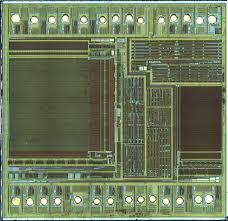
Crack Microcontroller PIC16LF677 Firmware Memory
Crack Microcontroller PIC16LF677 Firmware Memory needs to figure out the sequence of events for erasing a block of internal program memory location is:
1. Load EEADRH:EEADR with address of row being erased.
2. Set EEPGD bit to point to program memory; set WREN bit to enable writes and set FREE bit to enable the erase.
3. Disable interrupts.
4. Write 55h to EECON2.
5. Write AAh to EECON2.
6. Set the WR bit. This will begin the row erase cycle.
7. The CPU will stall for duration of the erase.
Flash program memory may only be written to if the destination address is in a segment of memory that is not write-protected, as defined in bits WRT1:WRT0 of the device Configuration Word (Register 12-1) by Extract MCU PIC18F2431 Program. Flash program memory must be written in four-word blocks.
A block consists of four words with sequential addresses, with a lower boundary defined by an address, where EEADR<1:0> = 00. At the same time, all block writes to program memory are done as write-only operations to facilitate the process of Unlock PIC16LF689 MCU Memory. The program memory must first be erased to Crack Microcontroller PIC16LF677 Firmware Memory. The write operation is edge-aligned and cannot occur across boundaries.
To write to the program memory, the data must first be loaded into the buffer registers. There are four 14-bit buffer registers and they are addressed by the low 2 bits of EEADR.
The following sequence of events illustrate how to perform a write to program memory from Recover MCU:
- Set the EEPGD and WREN bits in the EECON1 register
- Clear the FREE bit in EECON1
- Write address to EEADRH:EEADR
- Write data to EEDATH:EEDATA
- Write 55 to EECON2
- Write AA to EECON2
- Set WR bit in EECON 1
The user must follow the same specific sequence to initiate the write for each word in the program block by writing each program word in sequence when Clone PIC16C55 Microprocessor Flash Memory Program (00, 01, 10, 11).
This is not Sleep mode, as the clocks and peripherals will continue to run. After the erase cycle, the processor will resume operation with the third instruction after the EECON1 write instruction obtained from Clone ARM Microcontroller STM32F100C8.


