-
Product Categories
Live Support Chat


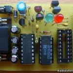
Crack Microcontroller dsPIC30F6015 Firmware
Crack Microcontroller dsPIC30F6015 secured memory and extract encrypted Firmware file from mcu dspic30f6015, break off IC security fuse bit;

The dsPIC DSC device contains a software stack. W15 is used as the Stack Pointer.
The Stack Pointer always points to the first available free word and grows from lower addresses towards higher addresses. It pre-decrements for stack pops and post-increments for stack pushes, as shown in Figure 3-9. Note that for a PC push during any CALL instruction, the MSB of the PC is zero-extended before the push, ensuring that the MSB is always clear.
There is a Stack Pointer Limit register (SPLIM) associated with the Stack Pointer. SPLIM is uninitialized at Reset. As is the case for the Stack Pointer, SPLIM<0> is forced to ‘0’, because all stack operations must be word-aligned. Whenever an Effective Address (EA) is generated using W15 as a source or destination pointer, the address thus generated is compared with the value in SPLIM if Crack Microcontroller dspic30f3012 hex.
If the contents of the Stack Pointer (W15) and the SPLIM register are equal and a push operation is performed, a stack error trap will not occur. The stack error trap will occur on a subsequent push operation. Thus, for example, if it is desirable to cause a stack error trap when the stack grows beyond address 0x2000 in RAM, initialize the SPLIM with the value, 0x1FFE.
The dsPIC30F6010A/6015 devices support Data RAM protection features which enable segments of RAM to be protected when used in conjunction with Boot and Secure Code Segment Security. BSRAM (Secure RAM segment for BS) is accessible only from the Boot Segment Flash code when enabled. SSRAM (Secure RAM segment for RAM) is accessible only from the Secure Segment Flash code when enabled.
The dual source operand DSP instructions (CLR, ED, EDAC, MAC, MPY, MPY.N, MOVSAC and MSC), also referred to as MAC instructions, utilize a simplified set of addressing modes to allow the user to effectively manipulate the data pointers through Register Indirect tables if Crack Microcontroller dspic30f3011 program.
The two source operand prefetch registers must be a member of the set {W8, W9, W10, W11}. For data reads, W8 and W9 will always be directed to the X RAGU and W10 and W11 will always be directed to the Y AGU. The Effective Addresses generated (before and after modification) must, therefore, be valid addresses within X data space for W8 and W9 and Y data space for W10 and W11.
Besides the various addressing modes outlined above, some instructions use literal constants of various sizes. For example, BRA (branch) instructions use 16-bit signed literals to specify the branch destination directly, whereas the DISI instruction uses a 14-bit unsigned literal field. In some instructions, such as ADD Acc, the source of an operand or result is implied by the opcode itself. Certain operations, such as NOP, do not have any operands.
Modulo Addressing is a method of providing an automated means to support circular data buffers using hardware. The objective is to remove the need for software to perform data address boundary checks when executing tightly looped code, as is typical in many DSP algorithms when Crack Microcontroller dspic30f4013 heximal.
In general, any particular circular buffer can only be configured to operate in one direction, as there are certain restrictions on the buffer start address (for incrementing buffers) or end address (for decrementing buffers) based upon the direction of the buffer. The only exception to the usage restrictions is for buffers which have a power-of-2 length. As these buffers satisfy the start and end address criteria, they may operate in a Bidirectional mode, (i.e., address boundary checks will be performed on both the lower and upper address boundaries).
Tags: crack microcontroller heximal archive,crack microcontroller heximal code,crack microcontroller heximal content,crack microcontroller heximal data,crack microcontroller heximal eeprom,crack microcontroller heximal file,crack microcontroller heximal firmware,crack microcontroller heximal information,crack microcontroller heximal memory,crack microcontroller heximal program