Crack Microcontroller AT89C51CC03 Flash
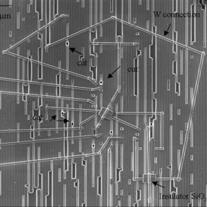
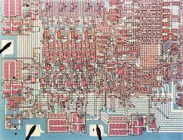
Crack Microcontroller AT89C51CC03 Flash memory and disable its security fuse bit, readout firmware from MCU’s memory to recover processor AT89C51CC03 flash content;
Each Port SFR operates via type-D latches, as illustrated in Figure 1 for Ports 3 and 4. A CPU “write to latch” signal initiates transfer of internal bus data into the type-D latch. A CPU “read latch” signal transfers the latched Q output onto the internal bus.
Similarly, a “read pin” signal transfers the logical level of the Port pin. Some Port data instructions activate the “read latch” signal while others activate the “read pin” signal. Latch instructions are referred to as Read-Modify-Write instructions if extract ic pic16c74 code.
Each I/O line may be independently programmed as input or output. Figure 1 shows the structure of Ports 1 and 3, which have internal pull-ups. An external source can pull the pin low. Each Port pin can be configured either for general-purpose I/O or for its alternate input output function.
To use a pin for general-purpose output, set or clear the corresponding bit in the Px register (x = 1,3 or 4). To use a pin for general-purpose input, set the bit in the Px register. This turns off the output FET drive before extract Microcontroller pic16c76 heximal.
To configure a pin for its alternate function, set the bit in the Px register. When the latch is set, the “alternate output function” signal controls the output level (see Figure 1). The operation of Ports 1, 3 and 4 is discussed further in the “quasi-Bidirectional Port Operation” section.
Ports 0 and 2 are used for general-purpose I/O or as the external address/data bus. Port 0, shown in Figure 3, differs from the other Ports in not having internal pull-ups. Figure 3 shows the structure of Port 2. An external source can pull a Port 2 pin low.
To use a pin for general-purpose output, set or clear the corresponding bit in the Px register (x = 0 or 2). To use a pin for general-purpose input, set the bit in the Px register to turn off the output driver FET. Some instructions read the latch data rather than the pin data. The latch based instructions read the data, modify the data and then rewrite the latch after extract chip pic16c71 code.
These are called “Read- Modify-Write” instructions. Below is a complete list of these special instructions (see Table ). When the destination operand is a Port or a Port bit, these instructions read the latch rather than the pin: write the new byte back to the latch.
These Read-Modify-Write instructions are directed to the latch rather than the pin in order to avoid possible misinterpretation of voltage (and therefore, logic) levels at the pin. For example, a Port bit used to drive the base of an external bipolar transistor can not rise above the transistor’s base-emitter junction voltage (a value lower than VIL). With a logic one written to the bit, attempts by the CPU to read the Port at the pin are misinterpreted as logic zero. A read of the latch rather than the pins returns the correct logic-one value.
Tags: crack microcontroller binary archive,crack microcontroller binary code,crack microcontroller binary content,crack microcontroller binary data,crack microcontroller binary eeprom,crack microcontroller binary file,crack microcontroller binary firmware,crack microcontroller binary information,crack microcontroller binary memory,crack microcontroller binary program


