-
Product Categories
Live Support Chat


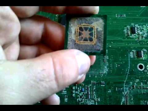
Crack Chip ATmega88A Program
Crack Chip ATmega88A fuse bit is a standard way to recover MCU Program from flash memory and make microcontroller ATmega88A copying;
- Power-up sequence:
Apply 4.5 – 5.5V between VCC and GND. Set PB5 and PB0 to “0” and wait at least 30 µs. Set PB3 to “0”. Wait at least 100 ns. Apply 12V to PB5 and wait at least 100 ns before changing PB0. Wait 8 µs before giving any instructions.
- The Flash array is programmed one byte at a time by supplying first the address, then the low and high data byte. The write instruction is self-timed; wait until the PB2 (RDY/BSY) pin goes high if clone mcu attiny26 binary.
- The EEPROM array is programmed one byte at a time by supplying first the address, then the data byte. The write instruction is self-timed; wait until the PB2 (RDY/BSY) pin goes high.
- Any memory location can be verified by using the Read instruction, which returns the contents at the selected address at serial output PB2.
- Power-off sequence:
Set PB3 to “0”.
Set PB5 to “0”.
Turn VCC power off.
When writing or reading serial data to the ATtiny15L, data is clocked on the 8th rising edge of the 16 external clock pulses needed to generate the internal clock after clone microcontroller atmega8 code.
Both th e program and data memory arrays can be programmed using the SPI bus while RESET is pulled to GND. The serial interface consists of pins SCK, MOSI (input) and MISO (output).
After RESET is set low, the Programming Enable instruction needs to be executed first before program/erase instructions can be executed.
For the EEPROM, an auto-erase cycle is provided within the self-timed write instruction and there is no need to first execute the Chip Erase instruction. The Chip Erase instruction turns the content of every memory location in both the program and EEPROM arrays into $FF if crack microcontroller atmega16l heximal.
The program and EEPROM memory arrays have separate address spaces: $0000 to $01FF for program memory and $000 to $03F for EEPROM memory. The device is clocked from the internal clock at the uncalibrated minimum frequency (0.8 – 1.6 MHz). The minimum low and high periods for the serial clock (SCK) input are defined as follows:
Low: > 2 MCU clock cycles
High: > 2 MCU clock cycles
Tags: crack chip binary archive,crack chip binary code,crack chip binary content,crack chip binary data,crack chip binary eeprom,crack chip binary file,crack chip binary firmware,crack chip binary heximal,crack chip binary information,crack chip binary memory,crack chip binary program


