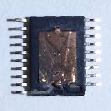
Clone PIC16C55 Microprocessor Flash Memory Program
The high performance of the PIC16C505 can be attributed to a number of architectural features commonly found in RISC microprocessors which is the reason why engineer want to apply and Clone PIC16C55 Microprocessor Flash Memory Program. To begin with, the PIC16C505 uses a Harvard architecture in which program and data are accessed on separate buses.
This improves bandwidth over traditional von Neumann architecture where program and data are fetched on the same bus after Crack Microchip PIC12F510 Locked Memory. Separating program and data memory further allows instructions to be sized differently than the 8-bit wide data word.
Instruction opcodes are 12-bits wide, making it possible to have all single word instructions. A 12-bit wide program memory access bus fetches a 12-bit instruction in a single cycle when Crack DSP Controller TMS320F243PGEA. A two-stage pipeline overlaps fetch and execution of instructions.
Consequently, all instructions (33) execute in a single cycle (200ns @ 20MHz) except for program branches. The PIC16C505 addresses 1K x 12 of program memory after Read Microcontroller PIC18F2515 Heximal. All program memory is internal. The PIC16C505 can directly or indirectly address its register files and data memory.
All special function registers, including the program counter, are mapped in the data memory for the purpose of Unlock IC PIC16C74B Binary. The PIC16C505 has a highly orthogonal (symmetrical) instruction set that makes it possible to carry out any operation on any register using any addressing mode. This symmetrical nature and lack of ‘special optimal situations’ make programming with the PIC16C505 simple yet efficient. In addition, the learning curve is reduced significantly before Reverse Engineering Microcontroller Code.


