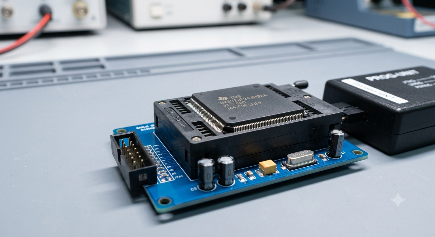
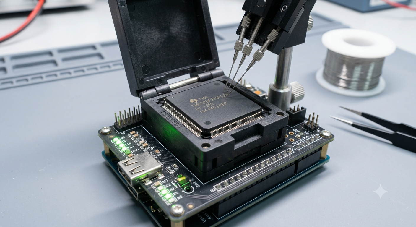
Crack DSP Controller TMS320F243PGEA
The texas instrument TMS320F243PGEA is a highly specialized 16-bit fixed-point dsp controller engineered primarily for real-time digital motor control, power conversion, and advanced industrial automation systems. Housed in a dense 144-pin LQFP package, this high-performance chip integrates an intelligent execution core with specialized pulse-width modulation modules, an onboard analog-to-digital converter, and a dedicated internal flash storage array. To protect sophisticated proprietary motor control logic and multi-layer communication protocols from competitive reverse-engineering, commercial product developers routinely activate the integrated chip-level code protection bits during production. This defensive measure transforms the processor into a locked state, initiating a dense protective hardware perimeter across the underlying silicon layout. This native security configuration prevents external standard emulators, logic analyzers, and factory debuggers from probing the internal memory registers, ensuring the proprietary digital architecture remains heavily guarded.
Team specializzati applicano incisione mediante fascio ionico focalizzato (FIB), micro-probing o tecniche di voltage-glitching altamente controllate direttamente sul substrato di silicio per neutralizzare in sicurezza i fusibili interni di protezione senza danneggiare le strutture principali della memoria.
La necessità commerciale di replicare completamente, clonare o recuperare in sicurezza il firmware del microcontrollore DSP Texas Instrument TMS320F243PG nel mercato industriale globale sta crescendo rapidamente a causa delle realtà logistiche e delle esigenze di continuità operativa.
The functional block diagram provides a high-level description of each component in the ’x240 DSP controller. The TMS320x240 devices are composed of three main functional units: a ’C2xx DSP core, internal memory, and peripherals. In addition to these three functional units, there are several system-level features of the ’x240 that are distributed. These system features include the memory map, device reset, interrupts, digital input/ output (I / O), clock generation, and low-power operation.
The TMS320x240 implements three separate address spaces for program memory, data memory, and I / O. Each space accommodates a total of 64K 16-bit words. Within the 64K words of data space, the 256 to 32K words at the top of the address range can be defined to be external global memory in increments of powers of two, as specified by the contents of the global memory allocation register (GREG). Access to global memory is arbitrated using the global memory bus request (BR) signal.

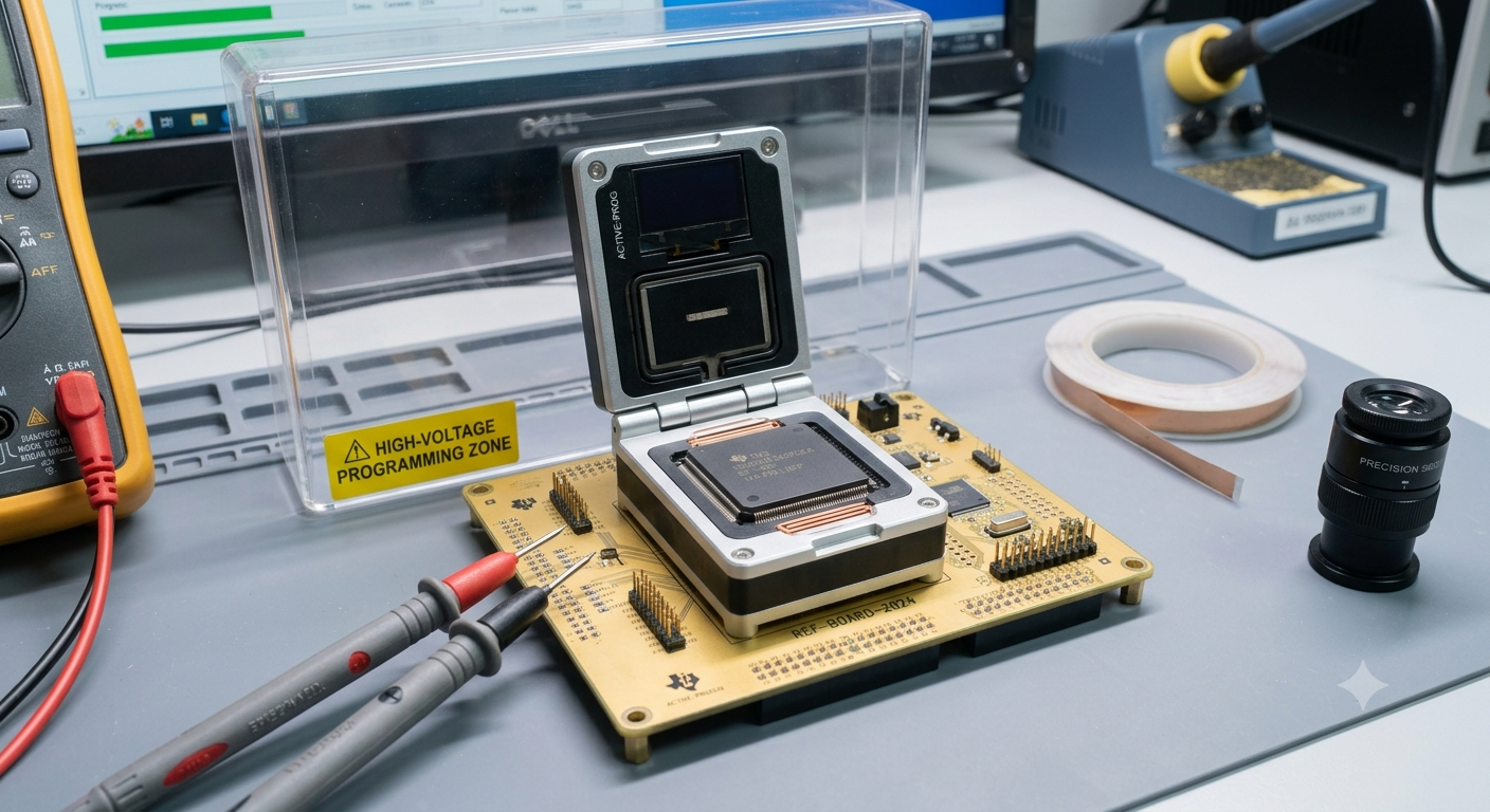
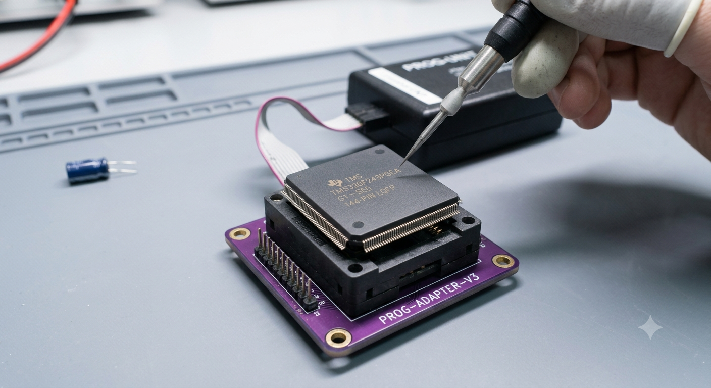
When an industrial engineering laboratory intends to crack, unlock, decrypt, or execute a secure readout from a protected processor, the operational process transitions from traditional software manipulation into precision microelectronics analysis. Bypassing a locked configuration to generate a completely flawless data dump requires highly localized, hardware-based circuit interrogation techniques that temporarily alter the chip’s logical boundaries. Specialized teams apply focused ion beam etching, micro-probing, or highly controlled voltage-glitching directly to the silicon substrate to safely neutralize the internal protection fuses without damaging the core memory structures. Once these underlying security flags are temporarily disabled, engineers can establish stable physical lines to interface directly with the on-chip storage arrays. This allows the engineering lab to copy and extract the deeply embedded logic structures, cleanly capturing the machine code and outputting it into an intact binary or heximal configuration layout for system validation.
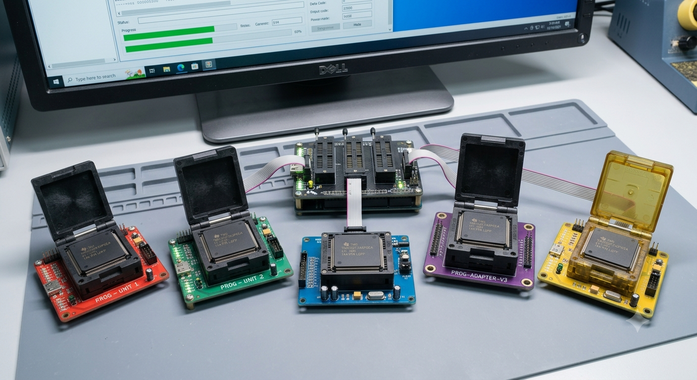
The commercial necessity to fully replicate, clone, or safely salvage active system firmware within the global industrial market is expanding rapidly due to logistical realities and operational survival. Thousands of heavy assembly lines, power sub-stations, and medical diagnostic platforms remain dependent on circuit boards managed by an obsolete or completely outdate digital controller. When an original hardware manufacturer goes out of business, or the foundational source code repository is permanently lost during corporate transitions, a single electronic breakdown can halt a critical infrastructure asset indefinitely. Extracting the active execution program from an operational backup module represents the only realistic method to prevent catastrophic downtime. Saving this vital operational data into a standardized archival file allows engineering teams to restore damaged components, manage unexpected component shortages, and safely clone legacy industrial controllers without investing years of labor and millions of dollars into ground-up software rebuilding.
Our precision microelectronics laboratory provides industrial end-users with highly specialized chip-level engineering, security bypass solutions, and complete code recovery services for high-density silicon architectures. Our specialized engineering staff maintains extensive technical experience navigating complex multi-layer chip layouts across a broad catalog of platforms, including specialized microcontrollers, standalone eeprom modules, high-capacity cpld arrays, and high-speed altera chip systems. By utilizing cleanroom-grade diagnostic platforms, we systematically work through localized physical security matrices to retrieve hidden device logic while protecting the original processing core. We deliver completely clean, production-ready firmware and software assets that can be written directly onto fresh replacement hardware. Partnering with our laboratory enables your technical teams to immediately reconstruct missing build histories, bypass lengthy development cycles, and securely protect your critical legacy infrastructure from unexpected system failures. Contact our technical team today to arrange a precise evaluation for your chip recovery project.