Unlock MCU ATTINY24 Program
Unlock MCU ATTINY24 and extract the Program from its flash and data of eeprom, the first step is to break IC protective cap and extract the firmware from its memory, the content of the Microcontroller will be same as original version;
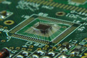
Unlock MCU ATTINY24 and extract the Program from its flash and data of eeprom, the first step is to break IC protective cap and extract the firmware from its memory, the content of the Microcontroller will be same as original version
If the code protection bit has not been programmed, the on-chip program memory can be read out for verification purposes. The first 64 locations and the last location (Reset vector) can be read, regardless of the code protection bit setting if attack ic microchip pic16f827.
Four memory locations are designated as ID locations where the user can store checksum or other code identification numbers. These locations are not accessible during normal execution, but are readable and writable during Program/Verify.
Use only the lower 4 bits of the ID locations and always program the upper 8 bits as ‘0’s. The ATTINY24 microcontrollers can be serially programmed while in the end application circuit.
This is simply done with two lines for clock and data, and three other lines for power, ground and the programming voltage. This allows customers to manufacture boards with unprogrammed devices and then program the microcontroller just before shipping the product when reverse engineering MCu chip c8051f340.
This also allows the most recent firmware or a custom firmware, to be programmed. The devices are placed into a Program/Verify mode by holding the GP1 and GP0 pins low while raising the MCLR (VPP) pin from VIL to VIHH (see programming specification).
GP1 becomes the programming clock and GP0 becomes the programming data. Both GP1 and GP0 are Schmitt Trigger inputs in this mode. After Reset, a 6-bit command is then supplied to the device.
Depending on the command, 16 bits of program data are then supplied to or from the device, depending if the command was a Load or a Read. For complete details of serial programming, please refer to the ATTINY24 Programming Specifications.
Tags: unlock mcu embedded archive,unlock mcu embedded code,unlock mcu embedded content,unlock mcu embedded data,unlock mcu embedded eeprom,unlock mcu embedded file,unlock mcu embedded firmware,unlock mcu embedded information,unlock mcu embedded memory,unlock mcu embedded program
