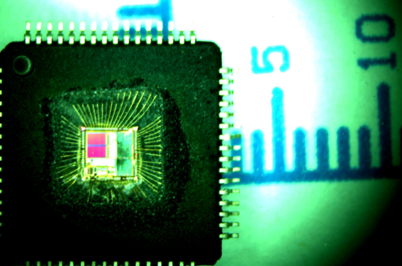
Unlock ATMEGA2560V Secured Microcontroller Heximal
Unlock ATMEGA2560V Secured Microcontroller Heximal will decode atmega2560v mcu firmware into the flash binary program and eeprom heximal data, the embedded firmware will be readout directly from atmega2560v original microprocessor;
SS: Slave Select input. When the SPI is enabled as a Slave, this pin is configured as an input regardless of the setting of DDB2. As a Slave, the SPI is activated when this pin is driven low. When the SPI is enabled as a Master, the data direction of this pin is controlled by DDB2.
When the pin is forced by the SPI to be an input, the pull-up can still be controlled by the PORTB2 bit. OC1B, Output Compare Match output: The PB2 pin can serve as an external output for the Timer/Counter1 Compare Match B when pull secured atmega1281 microcontroller software.
The PB2 pin has to be configured as an output (DDB2 set (one)) to serve this function. The OC1B pin is also the output pin for the PWM mode timer function.
OC1A, Output Compare Match output: The PB1 pin can serve as an external output for the Timer/Counter1 Compare Match A. The PB1 pin has to be configured as an output (DDB1 set (one)) to serve this function in the process of extracting atmega1281v mcu source code. The OC1A pin is also the output pin for the PWM mode timer function.