Texas Instrument DSP Microprocessor TMS320F28063 Binary Program Cloning
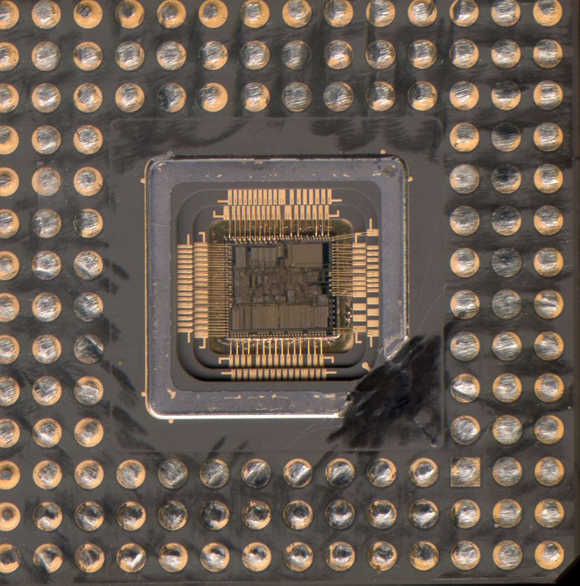
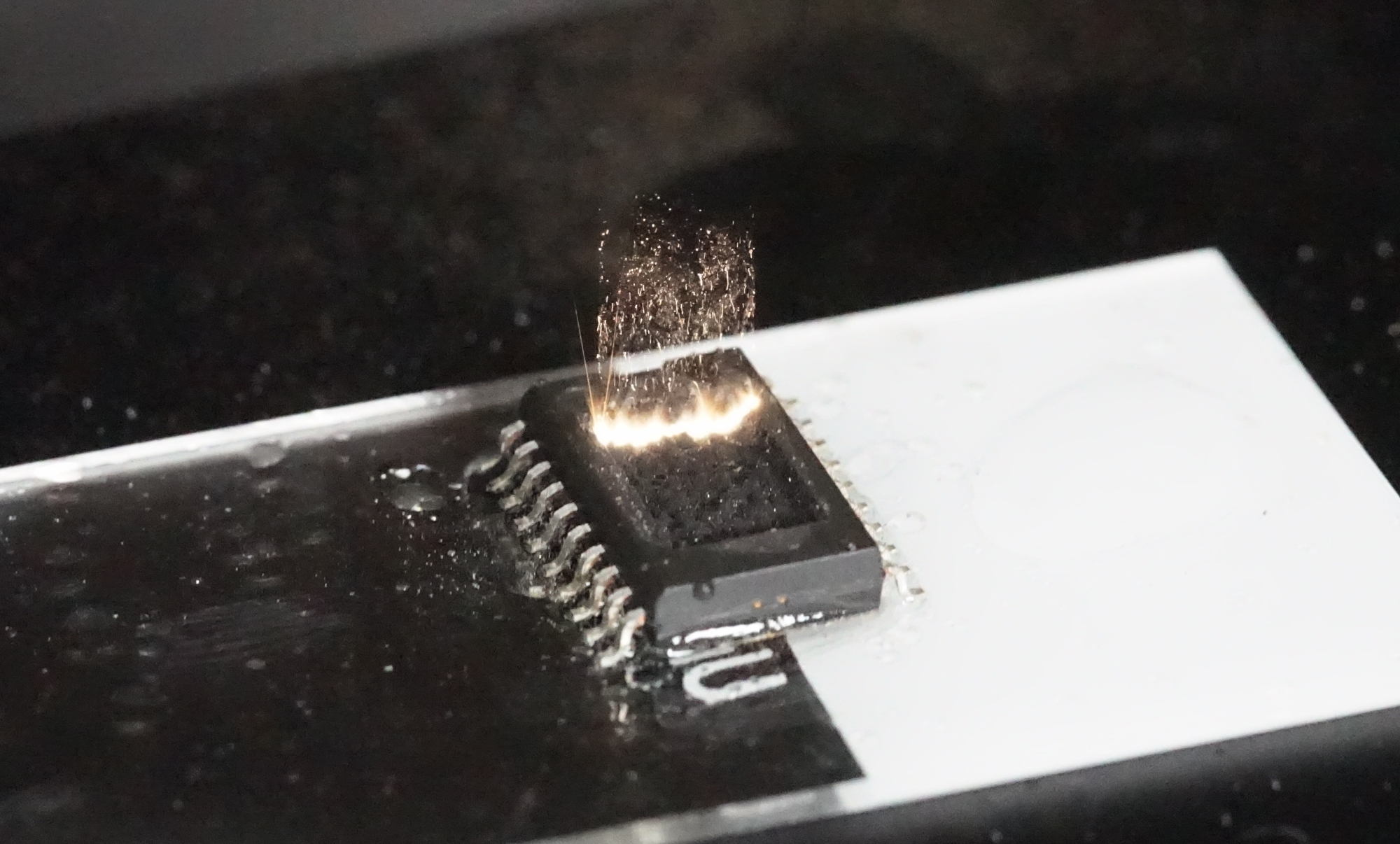
Texas Instrument DSP Microprocessor TMS320F28063 Binary Program Cloning needs to break dsp microcontroller tms320f28063 flash memory and extract locked firmware from MCU;
Each external interrupt can be enabled/disabled or qualified using positive, negative, or both positive and negative edge. For more information, see the TMS320x280x, 2801x, 2804x DSP System Control and Interrupts Reference Guide (literature number SPRU712).
This section describes the 280x oscillator, PLL and clocking mechanisms, the watchdog function and the low power modes. below Figure shows the various clock and reset domains in the 280x devices which are sharing the same functional blocks of cloning dsp microcontroller tms320f28044 flash memory content that will be discussed.
The user can select the type of input qualification for each GPIO pin through the GPxQSEL1/2 registers from four choices:
- Synchronization To SYSCLKOUT Only (GPxQSEL1/2 = 0, 0): This is the default mode of all GPIO pins at reset and it simply synchronizes the input signal to the system clock (SYSCLKOUT).
- Qualification Using Sampling Window (GPxQSEL1/2 = 0, 1 and 1, 0): In this mode the input signal, after synchronization to the system clock (SYSCLKOUT), is qualified by a specified number of cycles before the input is allowed to change.
- The sampling period is specified by the QUALPRD bits in the GPxCTRL register and is configurable in groups of 8 signals. The sampling period specifies a multiple of SYSCLKOUT cycles for sampling the input signal. The sampling window is either 3-samples or 6-samples wide and the output is only changed when ALL samples are the same (all 0s or all 1s) as shown in Figure 4-18 (for 6 sample mode).
- No Synchronization (GPxQSEL1/2 = 1,1): This mode is used for peripherals where synchronization is not required (synchronization is performed within the peripheral).
Due to the multilevel multiplexing that is required on the device, there may be cases where a peripheral input signal can be mapped to more then one GPIO pin.
Also, when an input signal is not selected, the input signal will default to either a 0 or 1 state, depending on the peripheral.