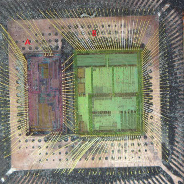
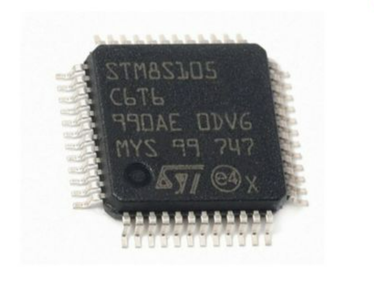
STM8S105C6T6 MCU Flash Memory Program Cloning
STM8S105C6T6 MCU Flash Memory Program Cloning starts from breaking stm8s105c6 micro cpu tamper resistance system and then extract embedded heximal code from stm8s105c6 flash memory;
Stresses above the absolute maximum ratings listed in Table 16: Voltage characteristics, Table 17: Current characteristics and Table 18: Thermal characteristics may cause permanent damage to the device. These are stress ratings only and functional operation of the device at these conditions is not implied when break mcu stm8s103k3u6 protection.
Exposure to maximum rating conditions for extended periods may affect the device’s reliability. The device’s mission profile (application conditions) is compliant with JEDEC JESD47 Qualification Standard, extended mission profiles are available on demand.
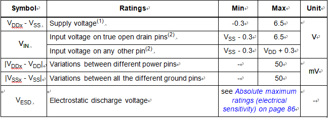
- All power (VDD) and ground (VSS) pins must always be connected to the external power supply
- IINJ(PIN) must never be exceeded. This is implicitly insured if VIN maximum is respected. If VIN maximum cannot be respected, the injection current must be limited externally to the IINJ(PIN) value. A positive injection is induced by VIN>VDD while a negative injection is induced by VIN<VSS after break stm8s103f3 mcu flash memory. For true open-drain pads, there is no positive injection current, and the corresponding VIN maximum must always be respected