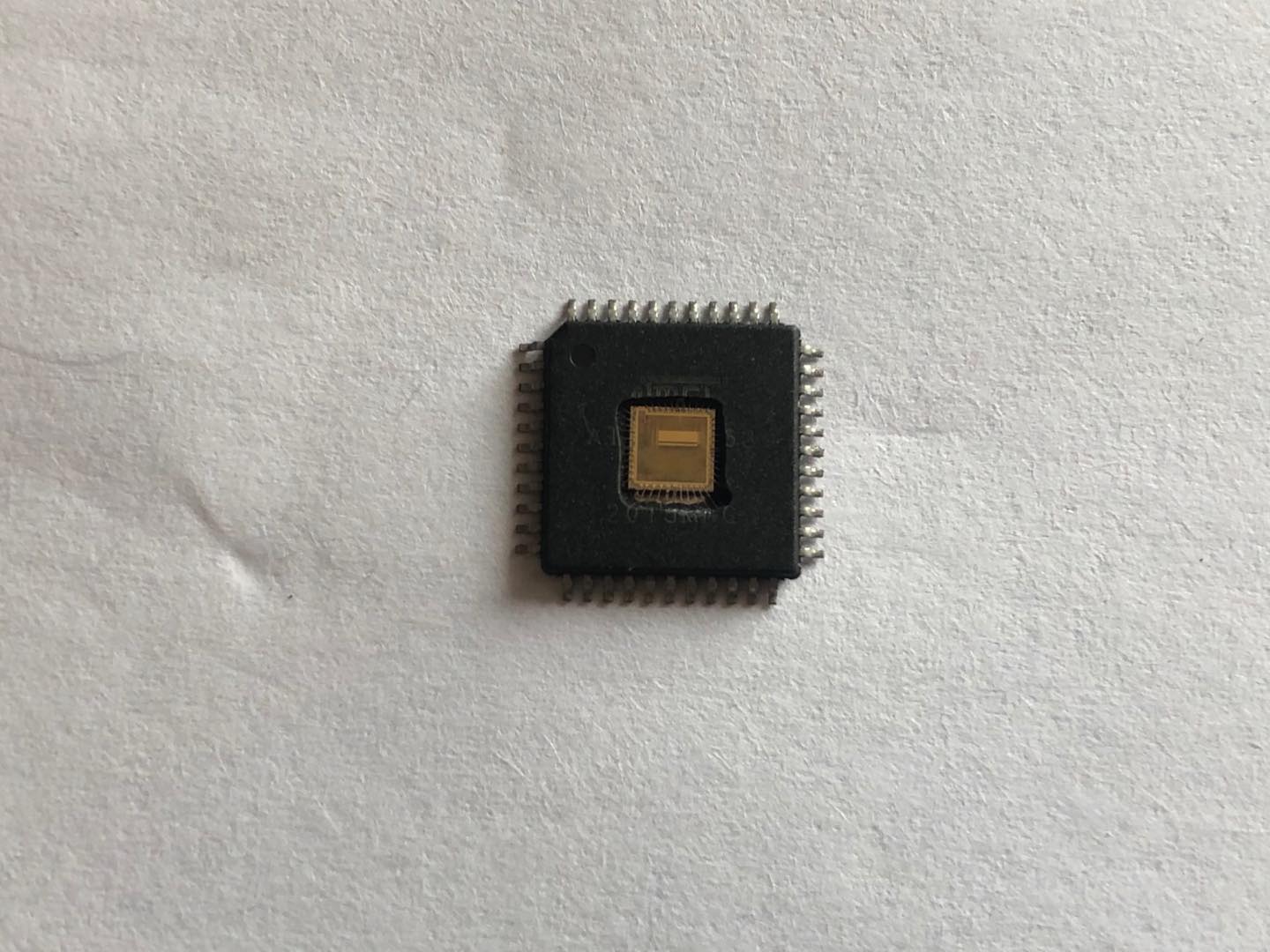
ST CPU SPC560P50L5 on chip code flash memory Cracking
ST CPU SPC560P50L5 on chip code flash memory Cracking will require focus ion beam technique to disable the security fuse bit which lock flash memory content inside microcontroller spc560p50l5, and then extract heximal file from un-secured microprocessor spc560p50l5 flash memory;
The SPC560P34/SPC560P40 provides 320 KB of programmable, non-volatile, flash memory. The non-volatile memory (NVM) can be used for instruction and/or data storage. The flash memory module is interfaced to the system bus by a dedicated flash memory controller.
It supports a 32-bit data bus width at the system bus port, and a 128-bit read data interface to flash memory. The module contains four 128-bit wide prefetch buffers only in the process of recovering automobile microprocessor spc560p40l3 flash memory firmware. Prefetch buffer hits allow no-wait responses. Normal flash memory array accesses are registered and are forwarded to the system bus on the following cycle, incurring two wait-states.
The flash memory module provides the following features:
- As much as 320 KB flash memory
- 6 blocks (32 KB + 2×16 KB + 32 KB + 32 KB + 128 KB) code flash memory
- 4 blocks (16 KB + 16 KB + 16 KB + 16 KB) data flash memory
- Full Read-While-Write (RWW) capability between code flash memory and data flash memory
- Four 128-bit wide prefetch buffers to provide single cycle in-line accesses (prefetch buffers can be configured to prefetch code or data or both)
- Typical flash memory access time: no wait-state for buffer hits, 2 wait-states for page buffer miss at 64 MHz
- Hardware managed flash memory writes handled by 32-bit RISC Krypton engine
- Hardware and software configurable read and write access protections on a per-master basis which can be applied for unlock spc560p34l3 32-bit SOC microcontroller.
- Configurable access timing allowing use in a wide range of system frequencies
- Multiple-mapping support and mapping-based block access timing (up to 31 additional cycles) allowing use for emulation of other memory types
- Software programmable block program/erase restriction control
- Erase of selected block(s)
- Read page sizes
- Code flash memory: 128 bits (4 words)
- Data flash memory: 32 bits (1 word)
- ECC with single-bit correction, double-bit detection for data integrity
- Code flash memory: 64-bit ECC
- Data flash memory: 32-bit ECC
- Embedded hardware program and erase algorithm
- Erase suspend and program abort
- Censorship protection scheme to prevent flash memory content visibility
- 6 blocks (32 KB + 2×16 KB + 32 KB + 32 KB + 128 KB) code flash memory
Hardware support for EEPROM emulation