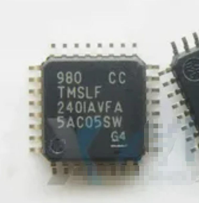
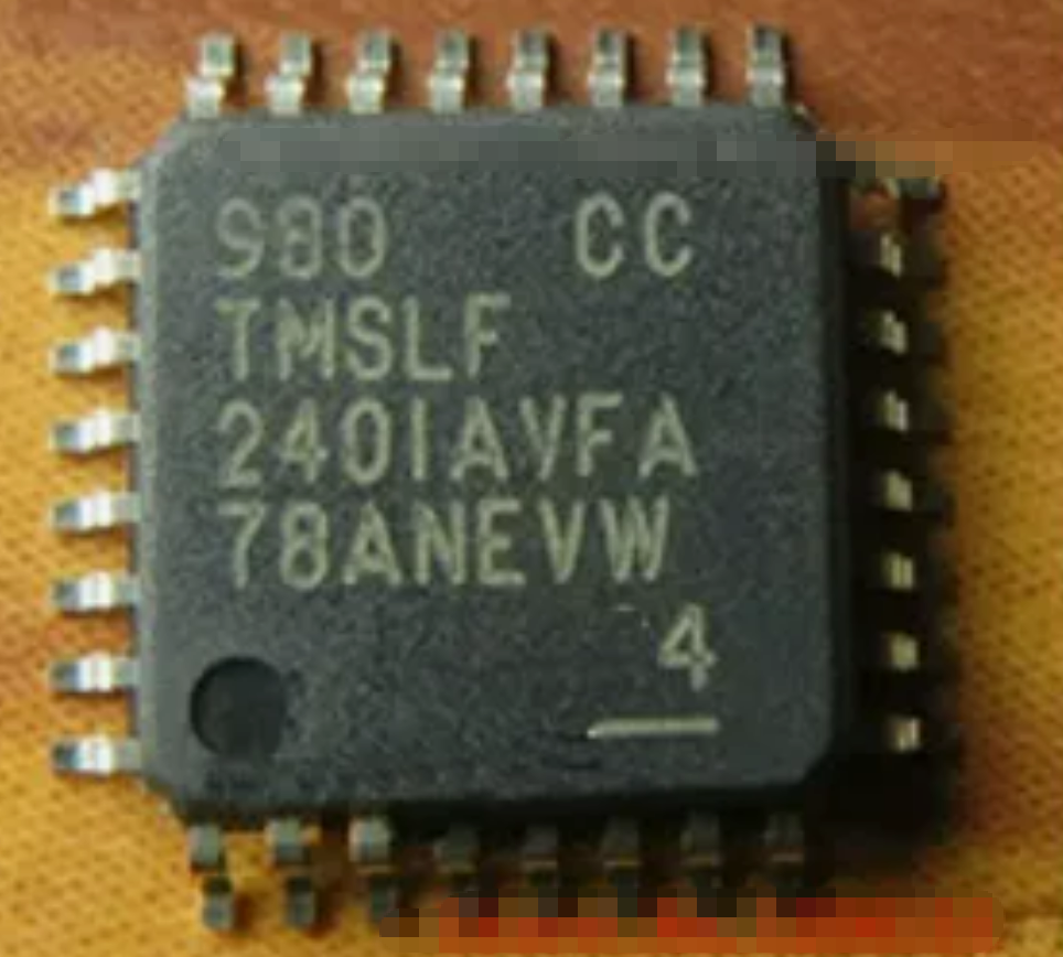
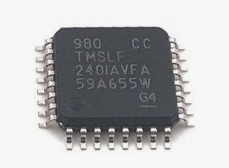
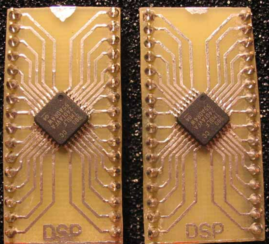
Reverse DSP IC Microcontroller Texas Instruments TMS320LF2401AVFA
Reverse DSP IC Microcontroller Texas Instruments TMS320LF2401AVFA has become a relevant topic in industrial repair, embedded system maintenance, and legacy equipment support. This device belongs to TI’s popular C2000 DSP family and is widely used in motion control, power conversion, automotive subsystems, and digital motor-driven platforms. Because of its real-time processing capability, PWM generators, and on-chip peripherals, it became a preferred option in high-precision automation equipment. However, its firmware is often secured, encrypted, and locked, making access to the internal program a technical challenge when replacement, recovery, or reverse engineering is required.
Many manufacturers deploying systems built on the TMS320LF2401AVFA MCU did not provide backup binary archives, original source code, or full documentation. Years later, when hardware fails, upgrading or restoring becomes nearly impossible without access to the embedded flash memory content. In these cases, the ability to readout, unlock, dump, or replicate the internal program becomes essential for continuity of production or system support.
We can Reverse DSP IC Microcontroller Texas Instruments TMS320LF2401AVFA, please view below chip features for your reference:
High-Performance Static CMOS Technology
− 25-ns Instruction Cycle Time (40 MHz)
− 40-MIPS Performance
− Low-Power 3.3-V Design
Based on TMS320C2xx DSP CPU Core
− Code-Compatible With F243/F241/C242
− Instruction Set and Module Compatible With F240 Flash (LF) and ROM (LC) Device Options
− LF240xA: LF2407A, LF2406A, LF2403A, LF2402A
− LC240xA: LC2406A, LC2404A, LC2403A, LC2402A
On-Chip Memory
− Up to 32K Words x 16 Bits of Flash EEPROM (4 Sectors) or ROM
− Programmable “Code-Security” Feature for the On-Chip Flash/ROM
− Up to 2.5K Words x 16 Bits of Data/Program RAM
− 544 Words of Dual-Access RAM
− Up to 2K Words of Single-Access RAM Boot ROM (LF240xA Devices)
− SCI/SPI Bootloader
Up to Two Event-Manager (EV) Modules (EVA and EVB), Each Includes:
− Two 16-Bit General-Purpose Timers
− Eight 16-Bit Pulse-Width Modulation (PWM) Channels Which Enable:
− Three-Phase Inverter Control
− Center- or Edge-Alignment of PWM Channels
− Emergency PWM Channel Shutdown With External PDPINTx Pin
− Programmable Deadband (Deadtime) Prevents Shoot-Through Faults
− Three Capture Units for Time-Stamping of External Events
− Input Qualifier for Select Pins
− On-Chip Position Encoder Interface Circuitry
− Synchronized A-to-D Conversion
− Designed for AC Induction, BLDC, Switched Reluctance, and Stepper Motor Control
− Applicable for Multiple Motor and/or Converter Control
External Memory Interface (LF2407A)
− 192K Words x 16 Bits of Total Memory:
64K Program, 64K Data, 64K I/O
Watchdog (WD) Timer Module
10-Bit Analog-to-Digital Converter (ADC)
− 8 or 16 Multiplexed Input Channels
− Selectable Twin 8-State Sequencers
Triggered by Two Event Managers
Controller Area Network (CAN) 2.0B Module
(LF2407A, 2406A, 2403A)
Serial Communications Interface (SCI)
16-Bit Serial Peripheral Interface (SPI)
(LF2407A, 2406A, LC2404A, 2403A)
Phase-Locked-Loop (PLL)-Based Clock
Generation
Up to 40 Individually Programmable, Multiplexed General-Purpose Input / Output (GPIO) Pins
Up to Five External Interrupts (Power Drive Protection, Reset, Two Maskable Interrupts)
Power Management:
− Three Power-Down Modes
− Ability to Power Down Each Peripheral Independently
Real-Time JTAG-Compliant Scan-Based
Emulation, IEEE Standard 1149.1† (JTAG)
Development Tools Include:
− Texas Instruments (TI) ANSI C Compiler, Assembler/ Linker, and Code Composer Studio Debugger
− Evaluation Modules
− Scan-Based Self-Emulation (XDS510)
− Broad Third-Party Digital Motor Control Support
Package Options
− 144-Pin LQFP PGE (LF2407A)
− 100-Pin LQFP PZ (2406A, LC2404A)
− 64-Pin TQFP PAG (LF2403A, LC2403A, LC2402A)
− 64-Pin QFP PG (2402A)
Extended Temperature Options (A and S)
− A: − 40°C to 85°C
− S: − 40°C to 125°C
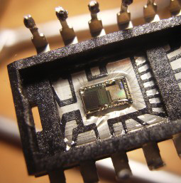
Working with this chip often involves detailed analysis of its internal EEPROM, protection registers, and fuse-based control mechanisms. While we do not publicly disclose the exact steps used to crack or decrypt the protection, the process may include non-invasive inspection, controlled interface access, or advanced reverse engineering techniques. The final objective is to successfully recover, restore, or copy the exact heximal program file, allowing the system to continue running identically or be migrated to an updated platform.
The difficulty level varies depending on revision, protection status, and condition of the hardware. Some samples require deeper decapsulation or specialized reading tools, while others can be accessed through indirect logic-behavior analysis.
Our team is experienced in handling DSP-grade microprocessors including TI TMS320 series, ensuring accurate duplicate or replicate program output without damaging the original chip. Whether the goal is maintenance, component substitution, or research-level evaluation, we provide stable technical support from secure data handling to final verified binary output.
For companies relying on industrial machinery, medical platforms, electric vehicle modules, energy systems, or robotics equipped with TMS320LF2401AVFA, this service ensures that functionality is preserved—even when original development resources are unavailable.