NXP Chip P89LPC970 Heximal Code Dumping
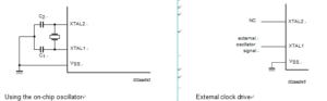
Clock Input Options and Recommended Capacitor Values for Oscillator, Shown in below Figure are the input and output of an internal inverting amplifier (XTAL1, XTAL2), which can be configured for use as an on-chip oscillator for NXP Chip P89LPC970 Heximal Code Dumping.
Oscillator characteristics
When driving the device from an external clock source, XTAL2 should be left disconnected and XTAL1 should be driven. At start-up, the external oscillator may encounter a higher capacitive load at XTAL1 due to interaction between the amplifier and its feedback capacitance to facilitate the process of NXP Chip P89LPC933 Memory Program Cloning. However, the capacitance will not exceed 15 pF once the external signal meets the VIL and VIH specifications.
NXP Chip P89LPC970 Heximal Code Dumping
The first two options are more reliable because the Watchdog timer is never disabled as in option #3. If the program counter ever goes astray, a match will eventually occur and cause an internal reset.
The second option is also not recommended if other PCA modules are being used. Remember, the PCA timer is the time base for all modules; changing the time base for other modules would not be a good idea if the situation comes to Clone Philip Chip LPC87LPC761 Heximal Code. Thus, in most applications the first solution is the best option.
To exit properly out of Power-down, the reset or external interrupt should not be executed before the VDD line is restored to its normal operating voltage. Be sure to hold VDD voltage long enough at its normal operating level for the oscillator to restart and stabilize (normally less than 10 ms).