
-
Product Categories
-
Live Support Chat


Hack CPLD IC Altera EPM240T100A MAX II Device
The Altera EPM240T100A, a member of the renowned MAX II family, is a highly versatile Complex Programmable Logic Device designed to offer low-cost, low-power control path processing across a broad spectrum of tech sectors. Frequently deployed in telecom infrastructure, industrial computing nodes, medical diagnostic interfaces, and high-performance consumer routing hardware, this non-volatile architecture integrates a distinct user FLASH sector along with high-density configuration MEMORY directly within its space-efficient IC footprint. To prevent competitor exploitation and safeguard complex internal logic routing matrices, hardware designers aggressively employ the component’s internal security fuses. This structural protectionism activates a heavily LOCKED security perimeter on the silicon level. The resulting PROTECTIVE hardware layer blocks boundary-scan utilities and standard testing equipment from surveying internal logic arrays, effectively neutralizing straightforward attempts to access the proprietary logic layout embedded inside the ALTERA Chip.
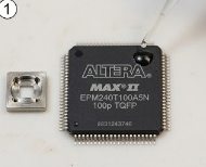
Quando il CPLD ALTERA EPM240T100A5N originale non è più disponibile oppure il repository principale del codice sorgente viene perso a causa della corruzione di dati legacy, l’estrazione del programma in esecuzione dal modulo ALTERA EPM240T100A5N ancora funzionante diventa l’unico modo realistico per mantenere la continuità operativa.
La conservazione di questi dati algoritmici essenziali in un archivio permanente consente ai team di sviluppo aziendali di duplicare componenti critici, sostituire schede logiche danneggiate e proteggere macchinari costosi da guasti operativi prolungati senza investire milioni nella completa riprogettazione dei sistemi.
When an engineering lab sets out to HACK, UNLOCK, DECRYPT, or safely CRACK an ENCRYPTED security block on a high-reliability programmable logic device or specialized microcontroller, the process centers on high-precision semiconductor recovery rather than simple software manipulation. Bypassing a LOCKED security fuse matrix to perform a complete code READOUT or direct data DUMP demands advanced micro-probing, localized voltage-margin optimization, or precise laser-ablation applied directly to the internal silicon architecture.
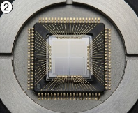
Cuando el CPLD ALTERA EPM240T100A5N original deja de estar disponible o el repositorio maestro del código fuente se pierde debido a corrupción de datos heredados, extraer el programa operativo desde un módulo ALTERA EPM240T100A5N superviviente y funcional se convierte en la única forma realista de mantener la continuidad del negocio.
Conservar estos datos algorítmicos críticos en un archivo permanente proporciona a los equipos corporativos de desarrollo los medios para clonar componentes esenciales, reemplazar placas lógicas dañadas y proteger maquinaria costosa frente a fallos operativos indefinidos sin comprometer millones en un rediseño completo del sistema.
This hardware-level neutralization temporarily suspends the chip’s security flags without disrupting the core gate arrays or logic blocks. Once the protective walls are lowered, technicians can interface with the internal storage nodes to systematically extract the hidden application files. This recovered structure is then precisely compiled into stable, uncorrupted BINARY or HEXIMAL data packets, ready for validation and physical duplication.
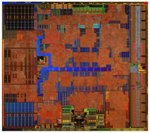
We can Hack CPLD IC Altera EPM240T100A MAX II Device, please view the IC chip features for your reference:
The MAX II CPLD has the following features:
Low-cost, low-power CPLD
Instant-on, non-volatile architecture
Standby current as low as 29 µA
Provides fast propagation delay and clock-to-output times
Provides four global clocks with two clocks available per logic array block (LAB)
UFM block up to 8 Kbits for non-volatile storage
MultiVolt core enabling external supply voltages to the device of either 3.3 V/2.5 V or 1.8 V
MultiVolt I/O interface supporting 3.3-V, 2.5-V, 1.8-V, and 1.5-V logic levels
Bus-friendly architecture including programmable slew rate, drive strength, bus-hold, and programmable pull-up resistors. Schmitt triggers enabling noise tolerant inputs (programmable per pin), I/Os are fully compliant with the Peripheral Component Interconnect Special, Interest Group (PCI SIG) PCI Local Bus Specification, Revision 2.2 for 3.3-V operation at 66 MHz.
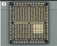
Когда оригинальный CPLD ALTERA EPM240T100A5N больше недоступен либо основной репозиторий исходного кода утрачен вследствие повреждения архивных данных, извлечение исполняемой программы из сохранившегося и работоспособного модуля ALTERA EPM240T100A5N становится единственным реалистичным способом поддержания непрерывности бизнеса.
Сохранение этих критически важных алгоритмических данных в постоянном архивном файле позволяет корпоративным инженерным группам клонировать ключевые компоненты, заменять повреждённые логические платы и защищать дорогостоящее оборудование от длительных простоев без необходимости тратить миллионы на полную переработку системы.
Supports hot-socketing
Built-in Joint Test Action Group (JTAG) boundary-scan test (BST) circuitry compliant with IEEE Std. 1149.1-1990
ISP circuitry compliant with IEEE Std. 1532
MAX II devices are available in space-saving FineLine BGA, Micro FineLine BGA, and thin quad flat pack (TQFP) packages (refer to Table 1–3 and 1–3). MAX II devices support vertical migration within the same package (for example, you can migrate between the EPM570, EPM1270, and EPM2210 devices in the 256-pin FineLine BGA package) for the purpose of Recovery IC CPLD Chip Xilinx XC9536XL-10VQG44C.
Vertical migration means that you can migrate to devices whose dedicated pins and JTAG pins are the same and power pins are subsets or supersets for a given package across device densities.
The largest density in any package has the highest number of power pins; you must lay out for the largest planned density in a package to provide the necessary power pins for migration. For I/O pin migration across densities, cross reference the available I/O pins using the device pin-outs for all planned densities of a given package type to identify which I/O pins can be migrated. The Quartus® II software can automatically cross-reference and place all pins for you when given a device migration list.
Quando o CPLD ALTERA EPM240T100A5N original deixa de existir ou o repositório principal do código-fonte é perdido devido à corrupção de dados legados, extrair o programa operacional de um módulo ALTERA EPM240T100A5N sobrevivente e funcional torna-se a única forma realista de manter a continuidade operacional.
Armazenar estes dados algorítmicos essenciais num ficheiro permanente permite às equipas corporativas de desenvolvimento clonar componentes críticos, substituir placas lógicas danificadas e proteger equipamentos de elevado valor contra falhas operacionais prolongadas sem investir milhões num redesenho completo do sistema.
The modern industrial market’s growing demand to REPLICATE, COPY, or extract these deeply embedded logic files is primarily driven by supply chain practicalities and asset preservation. A vast array of active factory lines, automated power sub-stations, and high-precision transport infrastructure run continuously on control systems governed by an OBSOLETE or completely OUTDATE programmable logic device or macrocell matrix. When the original equipment manufacturer dissolves, or the master SOURCE CODE repository is lost due to legacy data corruption, a single hardware breakdown can threaten an entire company’s operations. Extracting the execution PROGRAM from a surviving, functional module becomes the only realistic way to maintain business continuity. Securing this vital algorithmic DATA into a permanent archival FILE gives corporate development teams the means to clone critical components, replace damaged logic boards, and protect expensive machinery from indefinite operational failure without committing millions to total system redesigns.
Lorsque le CPLD ALTERA EPM240T100A5N d’origine disparaît ou que le dépôt principal du code source est perdu à cause de la corruption de données historiques, l’extraction du programme d’exécution depuis un module ALTERA EPM240T100A5N encore fonctionnel devient le seul moyen réaliste d’assurer la continuité des opérations.
La sécurisation de ces données algorithmiques essentielles dans un fichier d’archivage permanent offre aux équipes de développement d’entreprise les moyens de cloner des composants critiques, de remplacer des cartes logiques endommagées et de protéger des équipements coûteux contre des interruptions opérationnelles prolongées sans engager des millions dans une refonte complète du système.
Our advanced micro-engineering facility provides end-users with highly specialized hardware analysis, logic bypass workflows, and seamless code recovery solutions for critical semiconductor components. Our technical staff has extensive experience manipulating complex multi-layer chip architectures, working fluently across a diverse range of hardware platforms including specialized microcontrollers, standalone EEPROM modules, dense internal MEMORY chips, complex CPLD gate arrays, and high-speed DSP units. By operating cleanroom-grade analytical platforms, we systematically work through hardware locks to extract raw chip logic while preserving the operational integrity of your master device. We deliver fully verified, production-ready FIRMWARE files that can be directly written onto fresh target hardware, ensuring a smooth transition. Partnering with our lab allows your business to instantly recover lost design histories, avoid expensive development dead-ends, and keep your critical legacy infrastructure running smoothly. Contact our technical team today to schedule an evaluation of your hardware recovery project.