Extract Chip PIC18F8410 Code
Extract Chip PIC18F8410 Code from the memory like flash and eeprom, then copy the firmware into blank Microcontroller which will provide the same functions as original version;
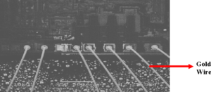
Extract Chip PIC18F8410 Code
The PIC18F8410 devices include an internal oscillator block, which generates two different clock signals; either can be used as the microcontroller’s clock source. This may eliminate the need for external oscillator circuits on the OSC1 and/or OSC2 pins.
The main output (INTOSC) is an 8 MHz clock source, which can be used to directly drive the device clock. It also drives a postscaler, which can provide a range of clock frequencies from 31 kHz to 4 MHz. The INTOSC output is enabled when a clock frequency from 125 kHz to 8 MHz is selected.
The other clock source is the internal RC oscillator (INTRC), which provides a nominal 31 kHz output. INTRC is enabled if it is selected as the device clock source; it is also enabled automatically when any of the following are enabled:
Power-up Timer
Fail-Safe Clock Monitor
Watchdog Timer
Two-Speed Start-up
These features are discussed in greater detail in
Section 23.0 “Special Features of the CPU” after Extract Chip.
The clock source frequency (INTOSC direct, INTRC direct or INTOSC postscaler) is selected by configuring the IRCF bits of the OSCCON register (Register 2-2).
2.6.1 INTIO MODES
Using the internal oscillator as the clock source eliminates the need for up to two external oscillator pins, which can then be used for digital I/O. Two distinct configurations are available:
· In INTIO1 mode, the OSC2 pin outputs FOSC/4, while OSC1 functions as RA7 for digital input and output. The internal oscillator block is calibrated at the factory to produce an INTOSC output frequency of 8.0 MHz.
The INTRC oscillator operates independently of the INTOSC source by reading the content out from MCU. Any changes in INTOSC across voltage and temperature are not necessarily reflected by changes in INTRC and vice versa.
The internal oscillator’s output has been calibrated at the factory, but can be adjusted in the user’s application. This is done by writing to the OSCTUNE register (Register 2-1). The tuning sensitivity is constant throughout the tuning range.
When the OSCTUNE register is modified, the INTOSC and INTRC frequencies will begin shifting to the new frequency. The INTRC clock will reach the new frequency within 8 clock cycles (approximately 8 * 32 µs = 256 µs). The INTOSC clock will stabilize within 1 ms. Code execution continues during this shift.
There is no indication that the shift has occurred. The OSCTUNE register also implements the INTSRC and PLLEN bits, which control certain features of the internal oscillator block. The INTSRC bit allows users to select which internal oscillator provides the clock source when the 31 kHz frequency option is selected.
This is covered in greater detail in Section 2.7.1
“Oscillator Control Register”.
The PLLEN bit controls the operation of the frequency multiplier, PLL, in internal oscillator modes.
Tags: extract chip source archive,extract chip source code,extract chip source content,extract chip source data,extract chip source eeprom,extract chip source file,extract chip source firmware,extract chip source information,extract chip source memory,extract chip source program