Dump Chip P89CV51RB2 Memory Data
Dump Chip P89CV51RB2 Memory Data need to know the programmable counter array working principle,
The Programmable Counter Array available on the 8XC51FX and 8XC51RX+ is a special 16-bit Timer that has five 16-bit capture/compare modules associated with it. Each of the modules can be programmed to operate in one of four modes: rising and/or falling edge capture, software timer, high-speed output, or pulse width modulator to facilitate the process of NXP P89LPC936 Embedded Firmware Restoration.
Dump Chip P89CV51RB2 Memory Data
Each module has a pin associated with it in port 1. Module 0 is connected to P1.3(CEX0) after Dump Chip P89CV51RB2 Memory Data, module 1 to P1.4(CEX1), etc. The basic PCA configuration is shown in below Figure.
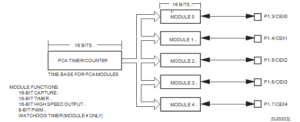
The PCA timer is a common time base for all five modules and can be programmed to run at: 1/12 the oscillator frequency, 1/4 the oscillator frequency, the Timer 0 overflow, or the input on the ECI pin (P1.2). The timer count source is determined from the CPS1 and CPS0 bits in the CMOD SFR as follows (see below Figure):
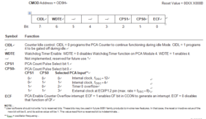
CMOD-PCA Counter Mode Register
CPS1 CPS0 PCA Timer Count Source
0 0 1/12 oscillator frequency
- 1 1/4 oscillator frequency
- 0 Timer 0 overflow
1 1 External Input at ECI pin
To use one of the PCA modules in the capture mode either one or both of the CCAPM bits CAPN and CAPP for that module must be set when Dump Chip P89CV51RB2 Memory Data. The external CEX input for the module (on port 1) is sampled for a transition.
When a valid transition occurs the PCA hardware loads the value of the PCA counter registers (CH and CL) into the module’s capture registers (CCAPnL and CCAPnH). If the CCFn bit for the module in the CCON SFR and the ECCFn bit in the CCAPMn SFR are set then an interrupt will be generated.