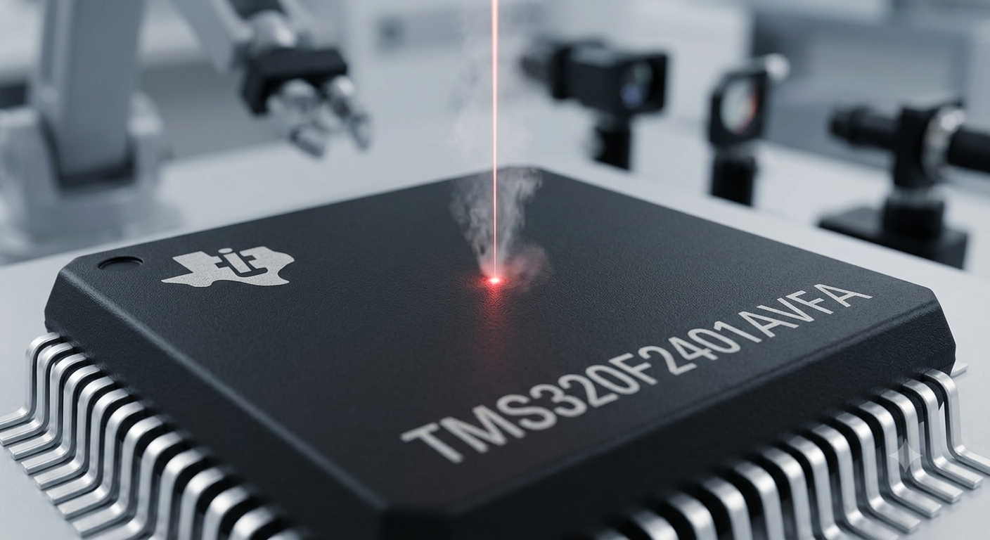
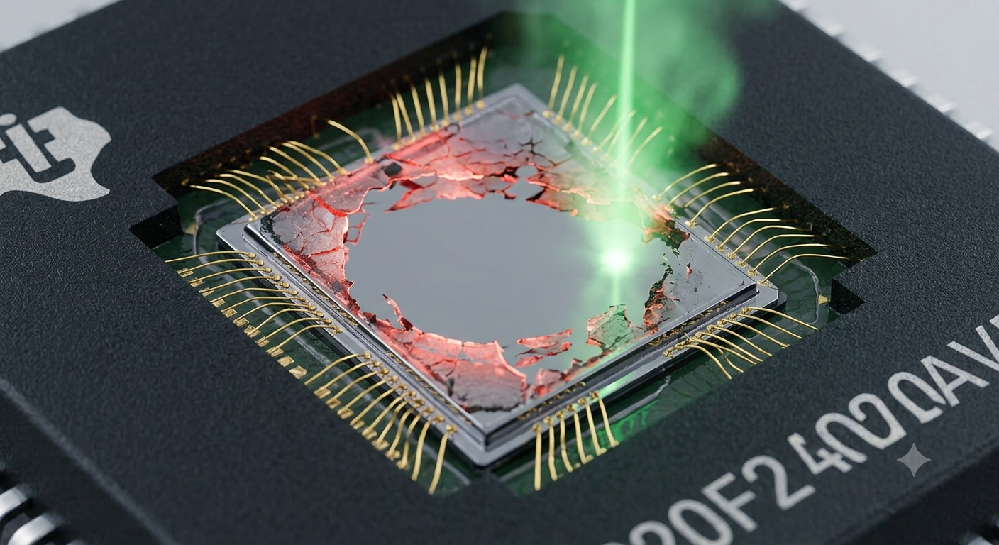
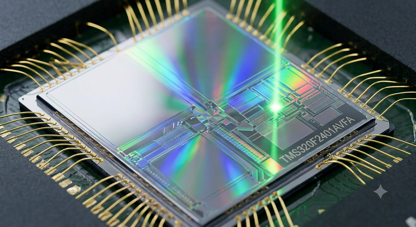
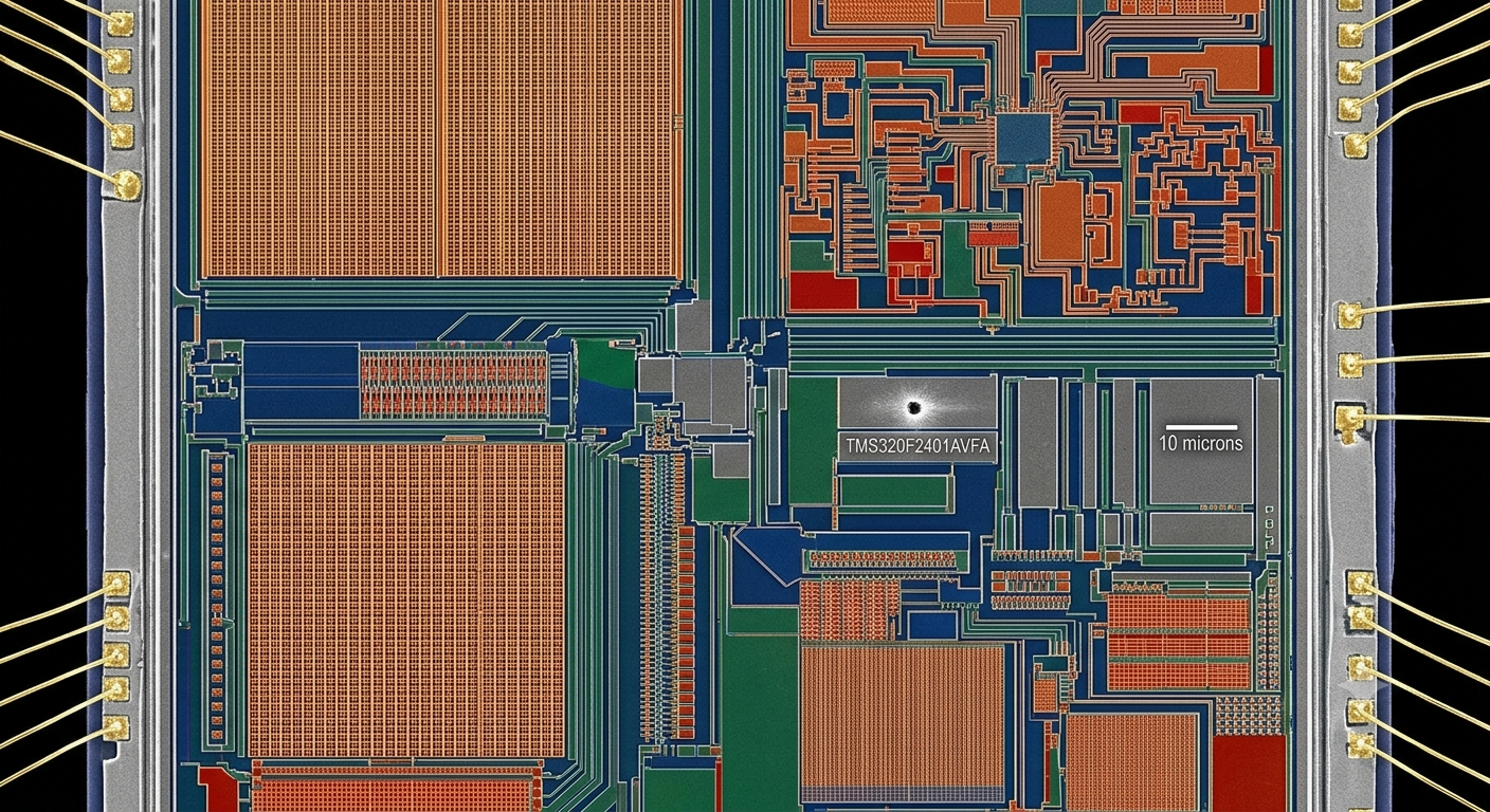
DSP Processor TMS320F2401AVFA Program Cloning
The texas instrument TMS320F2401AVFA is a highly specialized digital signal processor designed to provide cost-effective, high-efficiency motor control and power conversion capabilities across a broad spectrum of tech sectors. Frequently deployed in automotive electric power steering systems, industrial fan controllers, commercial HVAC units, and legacy uninterruptible power supplies, this compact dsp integrates a high-performance execution core with custom analog peripherals directly onto its physical silicon frame. To ensure proprietary control algorithms and custom communication profiles remain secure against competitive reverse-engineering, product developers routinely activate the hardware’s native security fuses during final assembly. This active protectionism locks configuration parameters to establish a strict boundary layer around the internal execution code. By implementing a protective electronic lock across the underlying layout, the chip effectively restricts external reading or scanning of its vital internal memory, ensuring the proprietary digital architecture remains heavily guarded against unauthorized inspection.
The F2401 has a total of 28 pins shared between primary functions and I/Os. These pins are divided into two groups:
Group1 — Primary functions shared with I/Os belonging to dedicated I/O ports, Port A, Port B, and Port C.
Group2 — Primary functions belonging to peripheral modules which also have a built-in I/O feature as a secondary function (for example, SCI, SPI, external interrupts, and PLL clock modules). The control structure for Group1 type shared I/O pins is shown in below Figure. The only exception to this configuration is the CLKOUT/IOPC1 pin. In below Figure, each pin has three bits that define its operation:
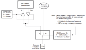
Mux control bit — this bit selects between the primary function (1) and I/O function (0) of the pin. I/O direction bit — if the I/O function is selected for the pin (mux control bit is set to 0), this bit determines whether the pin is an input (0) or an output (1). I/O data bit — if the I/O function is selected for the pin (mux control bit is set to 0) and the direction selected is an input, data is read from this bit; if the direction selected is an output, data is written to this bit. The mux control bit, I/O direction bit, and I/O data bit are in the I/O control registers.
When an electronics engineering laboratory handles a critical request to crack, unlock, decrypt, or execute a secure readout from a protected controller, the operational process transitions from traditional software manipulation into precision microelectronics analysis. Bypassing an encrypted or locked state to safely dump hidden device contents requires highly localized, hardware-based circuit interrogation techniques that temporarily alter the chip’s logical boundaries.
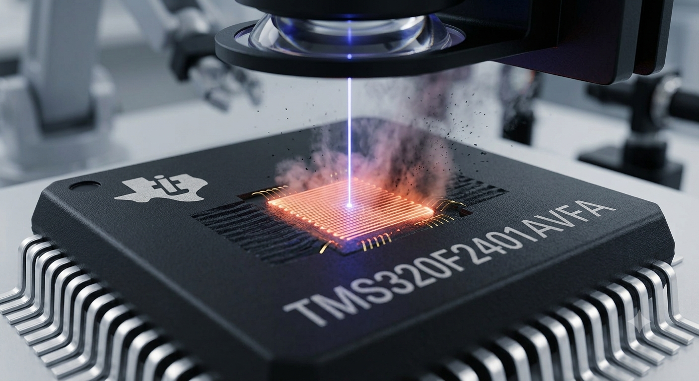
Technical groups utilize advanced laboratory workflows—such as precision voltage-glitching, localized thermal optimization, or micro-probing directly on the silicon substrate—to safely neutralize the internal protection flags without disrupting the core gate arrays. This intricate hardware-level neutralization opens a stable channel to communicate directly with the on-chip storage arrays, including the primary flash engine and independent eeprom data registers. Once the defensive perimeters are lowered, engineers can copy and extract the deeply embedded machine logic, cleanly capturing the application file and outputting it into an intact binary or heximal configuration layout for system validation.
The commercial necessity to fully replicate, clone, or safely salvage active system firmware within the global industrial market is expanding rapidly due to logistical realities and asset preservation. A vast number of active manufacturing lines, automated power sub-stations, and medical diagnostic platforms remain entirely dependent on circuit boards managed by an obsolete or completely outdate microchip. When an original hardware manufacturer goes out of business, or the master source code repository is permanently lost during corporate transitions, a single electronic breakdown can halt a critical infrastructure asset indefinitely.
Extracting the compiled program from an operational backup module represents the only realistic method to prevent catastrophic downtime. Saving this vital operational data into a standardized archival file allows engineering teams to restore damaged ic components, manage unexpected hardware shortages, and safely clone legacy industrial controllers without investing years of labor and millions of dollars into ground-up software rebuilding.
Our precision microelectronics laboratory provides industrial end-users with highly specialized chip-level engineering, security bypass solutions, and complete code recovery services for high-density silicon architectures. Our specialized engineering staff maintains extensive technical experience navigating complex multi-layer chip layouts across a broad catalog of platforms, including specialized microcontrollers, complex programmable logic devices (cpld), high-speed altera chip setups, and advanced processing nodes.
By utilizing cleanroom-grade diagnostic platforms, we systematically work through localized physical security matrices to retrieve hidden device logic while protecting the original processing core. We deliver completely clean, production-ready software packages that can be written directly onto fresh replacement hardware. Partnering with our laboratory enables your technical teams to immediately reconstruct missing build histories, bypass lengthy development cycles, and securely protect your critical legacy infrastructure from unexpected system failures. Contact our technical team today to arrange a precise evaluation for your chip recovery project.