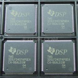
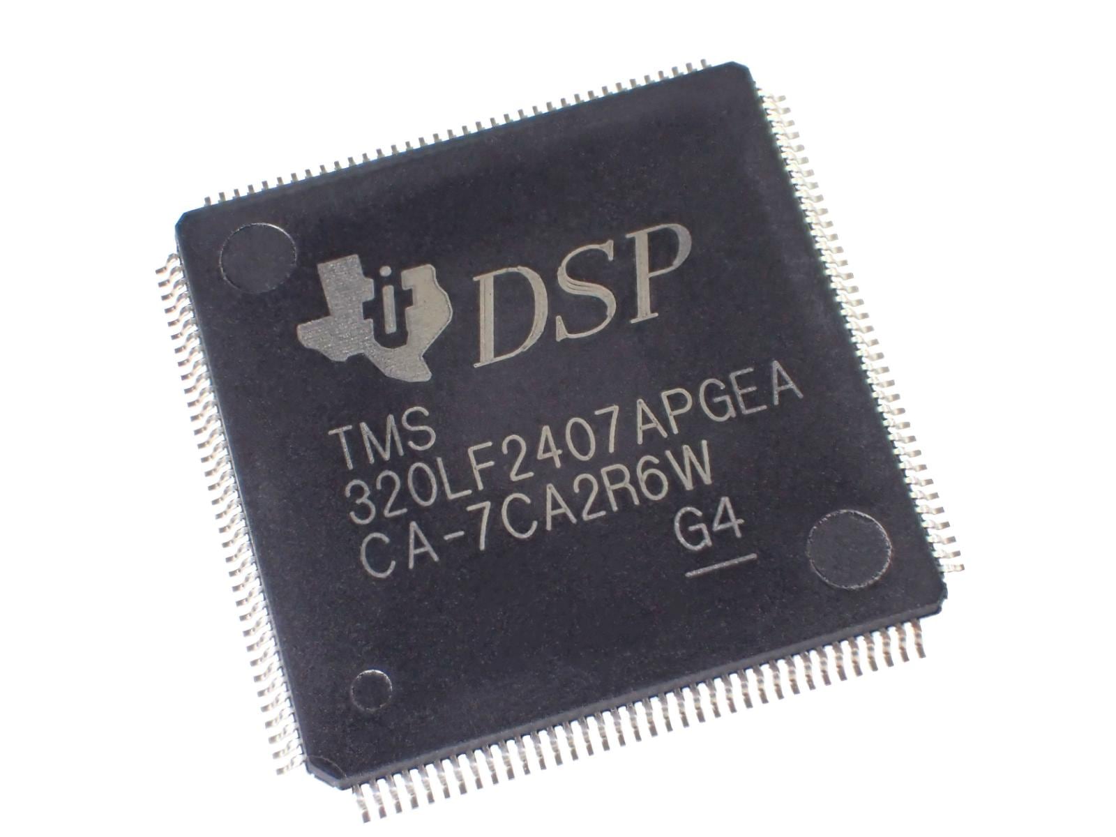
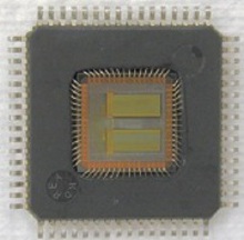
Decrypt Microcontroller IC DSP TMS320LF2407APGE
The TMS320LF2407APGE represents Texas Instruments’ advanced digital signal processor microcontroller specifically designed for real-time control applications. This sophisticated MCU combines a 32-bit DSP core with embedded flash and EEPROM memory, creating a powerful processing platform for demanding computational tasks. Unlike conventional ARM-based microcontrollers, this DSP chip employs specialized protective architectures including security fuses and encrypted memory access protocols that make reverse engineering particularly challenging. The device’s security mechanisms are fundamentally different from STM32 series, utilizing distinct secured memory partitioning and access control methodologies that require specialized approaches for firmware recovery attempts.
The TMS320LF2407APGE finds its primary applications in sectors requiring high-speed mathematical computation and real-time processing capabilities. In industrial motor control systems, this DSP microprocessor enables precise variable frequency drives and robotic motion controllers where the program contains proprietary motor control algorithms. The automotive industry utilizes these chips in advanced engine control units and anti-lock braking systems where processing sensor data in real-time is critical for vehicle safety. For power electronics applications, this microcomputer manages sophisticated power conversion systems and renewable energy inverters where the binary code contains valuable intellectual property related to power management algorithms. Additionally, the medical technology sector employs these processors in advanced diagnostic imaging equipment and patient monitoring systems where firmware reliability directly impacts device performance and safety.
Decrypting the secured firmware from a TMS320LF2407APGE microcontroller requires fundamentally different approaches compared to ARM-based processors. The process typically begins with analyzing the JTAG security fuses, which when locked, prevent standard debugging access to the memory contents. Technicians often employ reverse engineering techniques targeting the device’s security architecture, including attempts to decode the password protection mechanism that safeguards the flash and EEPROM regions. Specialized attack methods may involve power analysis techniques to decipher security keys or focused ion beam (FIB) work to physically bypass security fuses. For encrypted devices, professionals might use glitching attacks on the power supply or clock signals to break the security protocols and gain temporary access to the memory bus. Unlike the STM32 series, this DSP chip requires different voltage manipulation techniques and specialized equipment to recover the heximal code from protected memory regions.
We can Decrypt Microcontroller IC DSP TMS320LF2407APGE, please view the chip features for your reference:
High-Performance Static CMOS Technology
− 25-ns Instruction Cycle Time (40 MHz)
− 40-MIPS Performance
D Based on TMS320C2xx DSP CPU Core
− Code-Compatible With F243/F241/C242
− Instruction Set and Module Compatible With F240
D Flash (LF) and ROM (LC) Device Options
− LF240xA: LF2407A, LF2406A, LF2403A, LF2402A
− LC240xA: LC2406A, LC2404A, LC2403A, LC2402A
D On-Chip Memory
− Up to 32K Words x 16 Bits of Flash EEPROM (4 Sectors) or ROM
− Programmable “Code-Security” Feature for the On-Chip Flash/ROM
− Up to 2.5K Words x 16 Bits of Data/Program RAM
− 544 Words of Dual-Access RAM
− Up to 2K Words of Single-Access RAM D Boot ROM (LF240xA Devices)
− SCI/SPI Bootloader D Up to Two Event-Manager (EV) Modules
(EVA and EVB), Each Includes:
− Two 16-Bit General-Purpose Timers
− Eight 16-Bit Pulse-Width Modulation
− Three-Phase Inverter Control
− Center- or Edge-Alignment of PWM Channels
− Emergency PWM Channel Shutdown With External PDPINTx Pin
− Programmable Deadband (Deadtime) Prevents Shoot-Through Faults
− Three Capture Units for Time-Stamping of External Events
− Input Qualifier for Select Pins
− On-Chip Position Encoder Interface Circuitry
− Synchronized A-to-D Conversion
− Designed for AC Induction, BLDC,
Switched Reluctance, and Stepper Motor Control
− Applicable for Multiple Motor and/or Converter Control
The TMS320LF2407APGE presents unique difficulties for those attempting to hack or clone its firmware. The DSP architecture implements hardware-based security features including permanent security fuses that cannot be reversed once set, unlike the software-based protection found in many ARM microcontrollers. When locked, the device completely disables JTAG debugging access and blocks all memory read operations, returning invalid data or simply ignoring read commands. The chip’s advanced security circuitry can detect tampering attempts and may permanently erase critical program sections as a countermeasure against copying attempts. Physical obstacles include the LQFP-144 package with security mesh overlays that complicate microprobing attempts. Additionally, the DSP core architecture requires specialized knowledge to decrypt and decode the extracted binary even if successful memory access is achieved, as the instruction set and memory organization differ significantly from ARM processors.
D External Memory Interface (LF2407A)
− 192K Words x 16 Bits of Total Memory:
64K Program, 64K Data, 64K I/O D Watchdog (WD) Timer Module
D 10-Bit Analog-to-Digital Converter (ADC)
− 8 or 16 Multiplexed Input Channels
− 500-ns MIN Conversion Time
− Selectable Twin 8-State Sequencers
Triggered by Two Event Managers
D Controller Area Network (CAN) 2.0B Module
(LF2407A, 2406A, 2403A)
D Serial Communications Interface (SCI)
D 16-Bit Serial Peripheral Interface (SPI)
(LF2407A, 2406A, LC2404A, 2403A)
D Phase-Locked-Loop (PLL)-Based Clock Generation
D Up to 40 Individually Programmable, Multiplexed General-Purpose Input / Output (GPIO) Pins
D Up to Five External Interrupts (Power Drive Protection, Reset, Two Maskable Interrupts)
D Power Management:
− Three Power-Down Modes
− Ability to Power Down Each Peripheral Independently
D Real-Time JTAG-Compliant Scan-Based
Emulation, IEEE Standard 1149.1† (JTAG)
D Development Tools Include:
− Texas Instruments (TI) ANSI C Compiler, Assembler/ Linker, and Code Composer Studio Debugger
− Evaluation Modules
− Scan-Based Self-Emulation (XDS510)
− Broad Third-Party Digital Motor Control Support
D Package Options
− 144-Pin LQFP PGE (LF2407A)
− 100-Pin LQFP PZ (2406A, LC2404A)
− 64-Pin TQFP PAG (LF2403A, LC2403A, LC2402A)
− 64-Pin QFP PG (2402A)
D Extended Temperature Options (A and S)
− A: − 40°C to 85°C
− S: − 40°C to 125°C