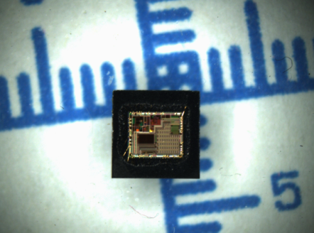
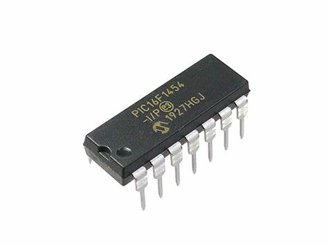
Decode Microcontroller PIC16F1454 Flash Code
Decode Microcontroller PIC16F1454 Flash Code from its flash memory, reverse engineering mcu pic16f1454 security fuse bit, and extract embedded firmware from pic16f1454 microprocessor flash and eeprom memory;
The value in the ADRESH/ADRESL registers is not modified for a Power-on Reset. The ADRESH/ADRESL registers will contain unknown data after a Power-on Reset. After the A/D module has been configured as desired, the selected channel must be acquired before the conversion is started.
The analog input channels must have their corresponding TRIS bits selected as an input. To determine acquisition time, see Section 17.1 “A/D Acquisition Requirements”. After this acquisition time has elapsed to clone pic16f1574 microcontroller flash heximal, the A/D conversion can be started. An acquisition time can be programmed to occur between setting the GO/DONE bit and the actual start of the conversion.
To do an A/D Conversion:
- Configure the A/D module:
- Configure analog pins, voltage reference and digital I/O (ADCON1)
- Select A/D input channel (ADCON0)
- Select A/D acquisition time (ADCON2)
- Select A/D conversion clock (ADCON2)
- Turn on A/D module (ADCON0)
- Configure A/D interrupt (if desired):
- Clear ADIF bit
- Set ADIE bit
- Set GIE bit
- Wait the required acquisition time (if required).
- Start conversion:
- Set GO/DONE bit (ADCON0 register)
- Wait for A/D conversion to complete, by either:
- Polling for the GO/DONE bit to be cleared OR
- Waiting for the A/D interrupt
- Read A/D Result registers (ADRESH:ADRESL); clear bit, ADIF, if required.
For the next conversion, go to step 1 or step 2, as required to unlock pic16f1574 microcontroller memory. The A/D conversion time per bit is defined as TAD to . A minimum wait of 2 TAD is required before the next acquisition starts.