Crack NXP P89C662 MCU Flash Memory
Through the expandable data ram address, the encrypted binary byte can be found effortlessly, and Crack NXP P89C662 MCU Flash Memory need to have some knowledge about this:
where R0 contains 0A0H, access the EXTRAM at address 0A0H rather than external memory. An access to external data memory locations higher than FFH (2FF for RD+) (i.e., 0100H to FFFFH) will be performed with the MOVX DPTR instructions in the same way as in the standard 80C51, so with P0 and P2 as data/address bus, and P3.6 and P3.7 as write and read timing signals. Refer to below Figure.
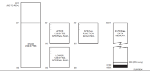
Internal and External Data Memory Address Space with EXTRAM = 0
With EXTRAM = 1, MOVX @Ri and MOVX @DPTR will be similar to the standard 80C51. MOVX @ Ri will provide an 8-bit address multiplexed with data on Port 0 and any output port pins can be used to output higher order address bits in order to Crack NXP P89C592 MCU Program Memory. This is to provide the external paging capability.
Crack NXP P89C662 MCU Flash Memory
MOVX @DPTR will generate a 16-bit address. Port 2 outputs the high-order eight address bits (the contents of DPH) while Port 0 multiplexes the low-order eight address bits (DPL) with data. MOVX @Ri and MOVX @DPTR will generate either read or write signals on P3.6 (#WR) and P3.7 (#RD) after Crack NXP P89C662 MCU Flash Memory.
The stack pointer (SP) may be located anywhere in the 256 bytes RAM (lower and upper RAM) internal data memory. The stack may not be located in the EXTRAM.