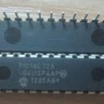
Crack IC dsPIC30F6014 Binary
Crack IC dsPIC30F6014 Binary means the firmware can be extracted from its memory and download to blank Microcontroller for a perfect cloning;
Crack IC dsPIC30F6014 Binary
In addition to adder/subtracter saturation, writes to data space may also be saturated but without affecting the contents of the source accumulator. The data space write saturation logic block accepts a 16-bit, 1.15 fractional value from the round logic block as its input, together with overflow status from the original source (accumulator) and the 16-bit round adder.
These are combined and used to select the appropriate 1.15 fractional value as output to write to data space memory. If the SATDW bit in the CORCON register is set, data (after rounding or truncation) is tested for overflow and adjusted accordingly, For input data greater than 0x007FFF, data written to memory is forced to the maximum positive 1.15 value, 0x7FFF.
For input data less than 0xFF8000, data written to memory is forced to the maximum negative 1.15 value, 0x8000. The MSb of the source (bit 39) is used to determine the sign of the operand being tested. If the SATDW bit in the CORCON register is not set, the input data is always passed through unmodified under all conditions.
The barrel shifter is capable of performing up to 16-bit arithmetic or logic right shifts, or up to 16-bit left shifts in a single cycle. The source can be either of the two DSP accumulators, or the X bus (to support multi-bit shifts of register or memory data). The shifter requires a signed binary value to determine both the magnitude (number of bits) and direction of the shift operation. A positive value will shift the operand right.
A negative value will shift the operand left. A value of ‘0’ will not modify the operand. The barrel shifter is 40 bits wide, thereby obtaining a 40-bit result for DSP shift operations and a 16-bit result for MCU shift operations. Data from the X bus is presented to the barrel shifter between bit positions 16 to 31 for right shifts, and bit positions 0 to 16 for left shifts.
The program address space is 4M instruction words. It is addressable by a 24-bit value from either the 23-bit PC, table instruction Effective Address (EA), or data space EA, when program space is mapped into data space as defined by Table 3-1. Note that the program space address is incremented by two between successive program words in order to provide compatibility with data space addressing.
This architecture fetches 24-bit wide program memory. Consequently, instructions are always aligned. However, as the architecture is modified Harvard, data can also be present in program space. There are two methods by which program space can be accessed: via special table instructions, or through the remapping of a 16K word program space page into the upper half of data space.
The TBLRDL and TBLWTL instructions offer a direct method of reading or writing the least significant word of any address within program space, without going through data space. The TBLRDH and TBLWTH instructions are the only method whereby the upper 8 bits of a program space word can be accessed as data after Crack IC.
The PC is incremented by two for each successive 24-bit program word. This allows program memory addresses to directly map to data space addresses. Program memory can thus be regarded as two 16-bit word wide address spaces, residing side by side, each with the same address range. TBLRDL and TBLWTL access the space which contains the least significant data word, and TBLRDH and TBLWTH access the space which contains the Most Significant Data Byte.
Figure 3-3 shows how the EA is created for table operations and data space accesses (PSV = 1). Here, P<23:0> refers to a program space word, whereas D<15:0> refers to a data space word. Data accesses to this area add an additional cycle to the instruction being executed, since two program memory fetches are required.
Note that the upper half of addressable data space is always part of the X data space. Therefore, when a DSP operation uses program space mapping to access this memory region, Y data space should typically contain state (variable) data for DSP operations, whereas X data space should typically contain coefficient (constant) data.
Although each data space address, 0x8000 and higher, maps directly into a corresponding program memory address (see Figure 3-6), only the lower 16 bits of the 24-bit program word are used to contain the data. The upper 8 bits should be programmed to force an illegal instruction to maintain machine robustness. Refer to the “dsPIC30F/33F Programmer’s Reference Manual” (DS70157) for details on instruction encoding.
Tags: crack ic embedded archive,crack ic embedded code,crack ic embedded content,crack ic embedded data,crack ic embedded eeprom,crack ic embedded file,crack ic embedded firmware,crack ic embedded information,crack ic embedded memory,crack ic embedded program