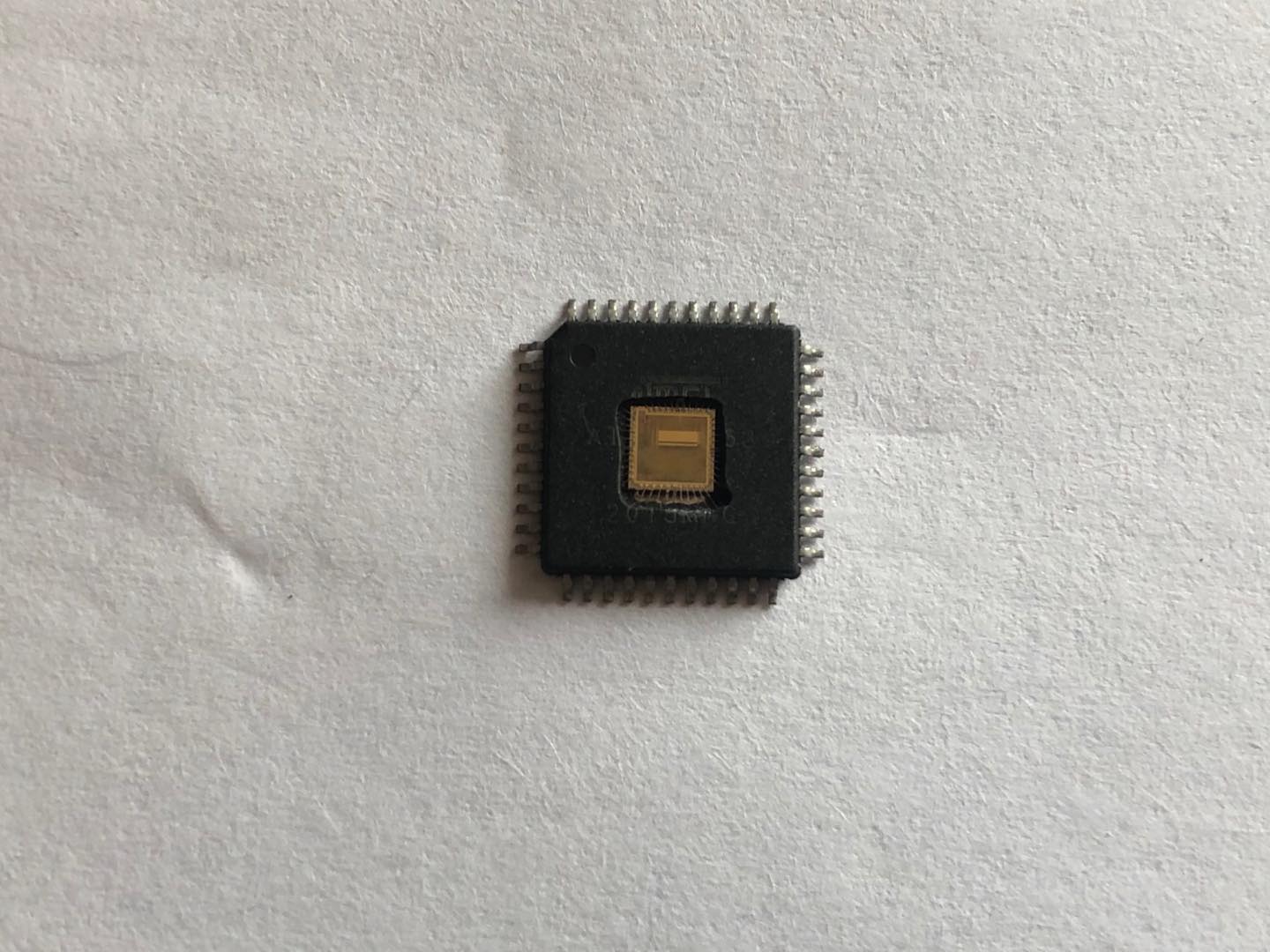
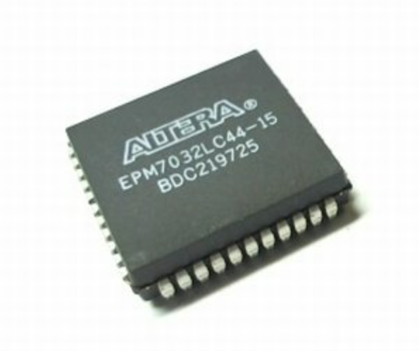
Crack Altera CPLD EPM7032LC44-10 Eeprom
Crack Altera CPLD EPM7032LC44-10 Eeprom FUSE BIT, and readout source code from altera cpld epm7032lc44 eeprom memory, and recover cpld epm7032lc44 pof or jed file from its eeprom memory;
The MAX 7000A device architecture supports the MultiVolt I/O interface feature, which allows MAX 7000A devices to connect to systems with differing supply voltages. MAX 7000A devices in all packages can be set for 2.5-V, 3.3-V, or 5.0-V I/O pin operation.
These devices have one set of VCC pins for internal operation and input buffers (VCCINT), and another set for I/O output drivers (VCCIO) and unlock the protection over epm7032aetc44 jed file. The VCCIO pins can be connected to either a 3.3-V or 2.5-V power supply, depending on the output requirements.
When the VCCIO pins are connected to a 2.5-V power supply, the output levels are compatible with 2.5-V systems. When the VCCIO pins are connected to a 3.3-V power supply, the output high is at 3.3 V and is therefore compatible with 3.3-V or 5.0-V systems which will bring convenience to cracking epm7032aelc44 eeprom memory.
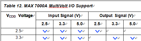
Devices operating with VCCIO levels lower than 3.0 V incur a slightly greater timing delay of tOD2 instead of tOD1. Inputs can always be driven by 2.5-V, 3.3-V, or 5.0-V signals.