CPLD Firmware Code Development Process
Hereby let’s talk about CPLD Firmware code Development Process, that is, the design process of the chip.
Most of the work of CPLD firmware code design and development will be completed on a computer.
CPLD Firmware Code Development
Open the integrated development software (Altera Max+pluxII) →
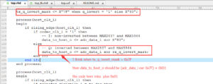
draw the schematic, write the hardware description language (VHDL, Verilog) →
compile →
give the input excitation signal of the logic circuit, perform simulation, check whether the logic output result is correct →
carry out the pin Input and output lock (64 input and output pins of 7128 can be set as needed) →
Generate code →
Transfer and store the firmware code in the CPLD chip through the download cable for MCU recovering. 7128 The chip has been led out, the digital tube, the answering switch, the indicator light, the buzzer are respectively connected to the chip board through the wire, and the power is tested.
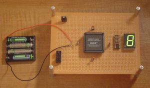
build a CPLD test debugging kit
When the answering switch is pressed, the corresponding indicator light should be on, correct. Later, after the referee gives extra points, see if the digital display bonus points are correct. If there is any problem, you can re-edit the schematic or hardware description language and improve the design.
After designing, such as mass production, you can directly copy firmware code into CPLD chips, that is, write code. If you want to make other designs on the chip, such as traffic light design, re-draw the schematic, or write the hardware description language, repeat the above work process and complete the design. This modified design is equivalent to the renovation of the house, which can be performed tens of thousands of times for the CPLD.