Clone Microcontroller NEC R5F21276JFP
Clone Microcontroller NEC R5F21276JFP means the firmware embedded inside this Microcontroller will be fully extracted and transfer to other blank MCU which will provide the same functions:
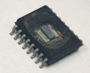
Clone Microcontroller NEC R5F21276JFP
CPU execution time
Operating Ambient Temperature
–40 to 85°C (D, J version) , -40 to 125°C (K version)
|
Item |
Specification |
|
|
CPU |
Number of fundamental instructions |
|
| Minimum instruction |
50 ns (f(XIN) = 20 MHz, VCC = 3.0 to 5.5 V) (other than K version) 62.5 ns (f(XIN) = 16 MHz, VCC = 3.0 to 5.5 V) (K version) 100 ns (f(XIN) = 10 MHz, VCC = 2.7 to 5.5 V) 200 ns (f(XIN) = 5 MHz, VCC = 2.2 to 5.5 V) (N, D version) |
|
| Operating mode |
Single-chip |
|
| Address space |
1 Mbyte |
|
| Memory capacity |
Refer to Table 1.3 Product Information for R8C/26 Group |
|
|
Peripheral Functions |
Ports |
I/O ports: 25 pins, Input port: 3 pins |
| LED drive ports |
I/O ports: 8 pins (N, D version) |
|
| Timers |
Timer RA: 8 bits × 1 channel (Each timer equipped with 8-bit prescaler) Timer RC: 16 bits × 1 channel (Input capture and output compare circuits) Timer RE: With real-time clock and compare match function (For J, K version, compare match function only.) |
|
| Serial interfaces |
2 channels (UART0, UART1) Clock synchronous serial I/O, UART |
|
| Clock synchronous |
1 channel 2 (1) I C bus Interface |
|
| LIN module |
Hardware LIN: 1 channel (timer RA, UART0) |
|
| A/D converter |
10-bit A/D converter: 1 circuit, 12 channels |
|
| Watchdog timer |
15 bits × 1 channel (with prescaler) Start-on-reset selectable |
|
| Interrupts |
Internal: 15 sources, External: 4 sources, Software: 4 sources, Priority levels: 7 levels |
|
| Clock generation |
3 circuits · XIN clock generation circuit (with on-chip feedback resistor) · On-chip oscillator (high speed, low speed) High-speed on-chip oscillator has a frequency adjustment function · XCIN clock generation circuit (32 kHz) (N, D version) · Real-time clock (timer RE) (N, D version) |
|
| Oscillation-stopped |
XIN clock oscillation stop detection function |
|
| Voltage detection |
On-chip |
|
| Power-on reset circuit |
On-chip |
|
|
Electrical Characteristics |
Supply voltage |
VCC = 3.0 to 5.5 V (f(XIN) = 20 MHz) (other than K version) VCC = 3.0 to 5.5 V (f(XIN) = 16 MHz) (K version) VCC = 2.7 to 5.5 V (f(XIN) = 10 MHz) VCC = 2.2 to 5.5 V (f(XIN) = 5 MHz) (N, D version) |
| Current consumption |
Typ. 10 mA (VCC = 5.0 V, f(XIN) = 20 MHz) Typ. 6 mA (VCC = 3.0 V, f(XIN) = 10 MHz) Typ. 2.0 µA (VCC = 3.0 V, wait mode (f(XCIN) = 32 kHz) Typ. 0.7 µA (VCC = 3.0 V, stop mode) |
|
|
Flash Memory |
Programming and erasure voltage |
VCC = 2.7 to 5.5 V |
| Programming and |
100 times |
|
|
Operating Ambient Temperature |
-20 to 85°C (N version) |
|
| (2) (2) | ||
|
Package |
32-pin molded-plastic LQFP |
|
|
Item |
Specification |
|
|
CPU |
Number of fundamental instructions |
89 instructions |
| Minimum instruction |
50 ns (f(XIN) = 20 MHz, VCC = 3.0 to 5.5 V) (other than K version) 62.5 ns (f(XIN) = 16 MHz, VCC = 3.0 to 5.5 V) (K version) 100 ns (f(XIN) = 10 MHz, VCC = 2.7 to 5.5 V) 200 ns (f(XIN) = 5 MHz, VCC = 2.2 to 5.5 V) (N, D version) |
|
| Operating mode |
Single-chip |
|
| Address space |
1 Mbyte |
|
| Memory capacity |
Refer to Table 1.4 Product Information of R8C/27 Group |
|
|
Peripheral Functions |
Ports |
I/O ports: 25 pins, Input port: 3 pins |
| LED drive ports |
I/O ports: 8 pins (N, D version) |
|
| Timers |
Timer RA: 8 bits × 1 channel Timer RB: 8 bits × 1 channel (Each timer equipped with 8-bit prescaler) Timer RC: 16 bits × 1 channel (Input capture and output compare circuits) Timer RE: With real-time clock and compare match function (For J, K version, compare match function only.) |
|
| Serial interfaces |
2 channels (UART0, UART1) Clock synchronous serial I/O, UART |
|
| Clock synchronous |
1 channel 2 (1) I C bus Interface Clock synchronous serial I/O with chip select |
|
| LIN module |
Hardware LIN: 1 channel (timer RA, UART0) |
|
| A/D converter |
10-bit A/D converter: 1 circuit, 12 channels |
|
| Watchdog timer |
15 bits × 1 channel (with prescaler) Start-on-reset selectable |
|
| Interrupts |
Internal: 15 sources, External: 4 sources, Software: 4 sources, Priority levels: 7 levels |
|
| Clock generation |
3 circuits · XIN clock generation circuit (with on-chip feedback resistor) · On-chip oscillator (high speed, low speed) High-speed on-chip oscillator has a frequency adjustment function · XCIN clock generation circuit (32 kHz) (N, D version) · Real-time clock (timer RE) (N, D version) |
|
| Oscillation-stopped |
XIN clock oscillation stop detection function |
|
| Voltage detection circuit |
On-chip |
|
| Power-on reset circuit |
On-chip |
|
|
Electrical Characteristics |
Supply voltage |
VCC = 3.0 to 5.5 V (f(XIN) = 20 MHz) (other than K version) VCC = 3.0 to 5.5 V (f(XIN) = 16 MHz) (K version) VCC = 2.7 to 5.5 V (f(XIN) = 10 MHz) VCC = 2.2 to 5.5 V (f(XIN) = 5 MHz) (N, D version) |
| Current consumption |
Typ. 10 mA (VCC = 5.0 V, f(XIN) = 20 MHz) Typ. 6 mA (VCC = 3.0 V, f(XIN) = 10 MHz) Typ. 2.0 µA (VCC = 3.0 V, wait mode (f(XCIN) = 32 kHz) Typ. 0.7 µA (VCC = 3.0 V, stop mode) |
|
|
Flash Memory |
Programming and erasure voltage |
VCC = 2.7 to 5.5 V |
| Programming and |
10,000 times (data flash) |
|
| 1,000 times (program ROM) | ||
|
Operating Ambient Temperature |
-20 to 85°C (N version) |
|
| (2) (2) | ||
|
Package |
32-pin molded-plastic LQFP |
|