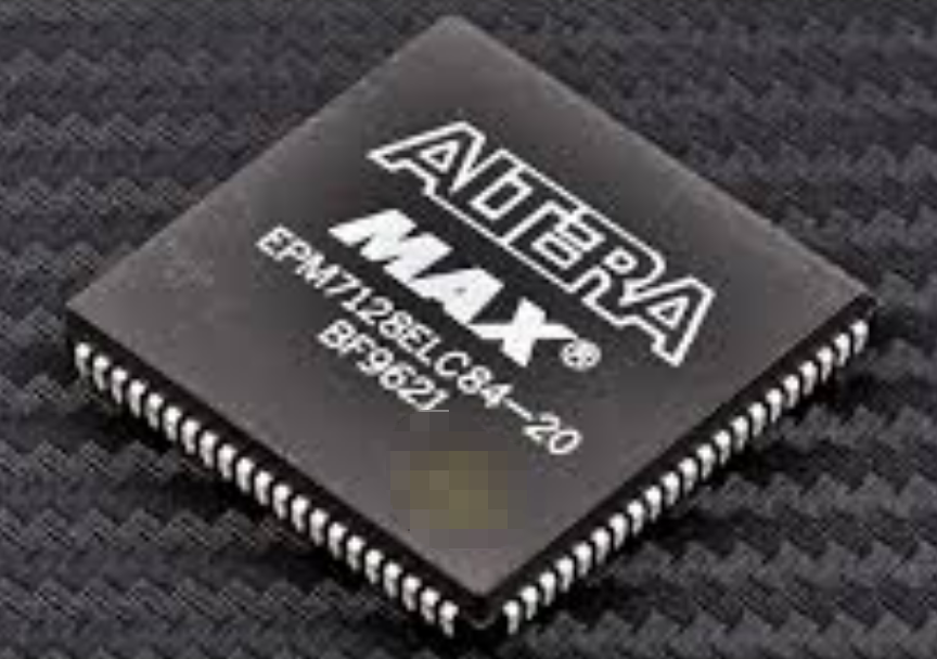
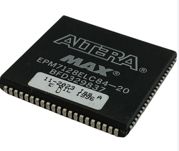
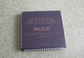
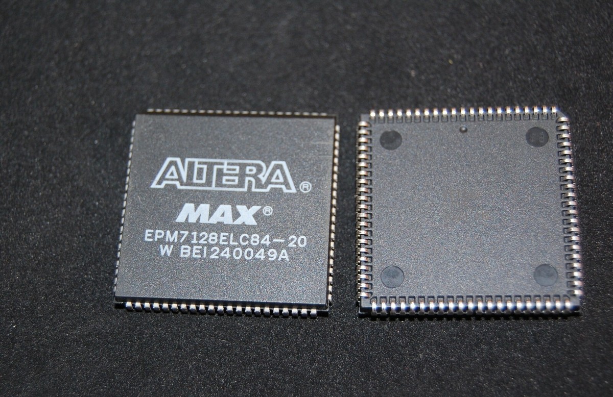
Attack PLD IC Altera EPM7128ELC84-10
Attack PLD IC Altera EPM7128ELC84-10 refers to the deep technical process of understanding, extracting, and reconstructing the internal configuration of Altera’s classic MAX7000-series PLDs. These devices are widely used in industrial controllers, communication interfaces, and embedded instrumentation, where the internal configuration behaves much like immutable hardware firmware, forming the logic backbone of timing, gating, and combinational control functions.
We can Attack PLD IC Altera EPM7128ELC84-10, please view below IC features for your reference:
High-performance, EEPROM-based programmable logic devices
(PLDs) based on second-generation MAX® architecture
5.0-V in-system programmability (ISP) through the built-in
IEEE Std. 1149.1 Joint Test Action Group (JTAG) interface available in
The EPM7128ELC84-10 is a CPLD-class chip featuring deterministic propagation timing, stable non-volatile storage, and robust I/O structures. Engineers often encounter these devices in:
- Legacy telecom switching and routing hardware
- Industrial automation modules
- Motor control and actuator interfaces
- Measurement and diagnostic equipment
- Aerospace and defense subsystems that require deterministic logic
In these applications, the PLD’s configuration binary is equivalent to hardware-level source code, and recovering this program or archive becomes essential when migrating, repairing, or updating designs where original design files were lost.
– ISP circuitry compatible with IEEE Std. 1532
Includes 5.0-V MAX 7000 devices and 5.0-V ISP-based MAX 7000S devices
Built-in JTAG boundary-scan test (BST) circuitry in MAX 7000S devices with 128 or more macrocells
Complete EPLD family with logic densities ranging from 600 to 5,000 usable gates (see Tables 1 and 2) 5-ns pin-to-pin logic delays with up to 175.4-MHz counter frequencies (including interconnect)
PCI-compliant devices available
Open-drain output option in MAX 7000S devices
Programmable macrocell flipflops with individual clear, preset, clock, and clock enable controls
Programmable power-saving mode for a reduction of over 50% in each macrocell
Configurable expander product-term distribution, allowing up to 32 product terms per macrocell 44 to 208 pins available in plastic J-lead chip carrier (PLCC), ceramic pin-grid array (PGA), plastic quad flat pack (PQFP), power quad flat pack (RQFP), and 1.0-mm thin quad flat pack (TQFP) packages Programmable security bit for protection of proprietary designs 3.3-V or 5.0-V operation.
– MultiVoltTM I/O interface operation, allowing devices to interface with 3.3-V or 5.0-V devices (MultiVolt I/O operation is not available in 44-pin packages)
– Pin compatible with low-voltage MAX 7000A and MAX 7000B devices
Enhanced features available in MAX 7000E and MAX 7000S devices
– Six pin- or logic-driven output enable signals
– Two global clock signals with optional inversion
– Enhanced interconnect resources for improved routability
– Fast input setup times provided by a dedicated path from I/O pin to macrocell registers
– Programmable output slew-rate control
Software design support and automatic place-and-route provided by Altera’s development system for Windows-based PCs and Sun SPARCstation, and HP 9000 Series 700/800 workstations Additional design entry and simulation support provided by EDIF 2 0 0 and 3 0 0 netlist files, library of parameterized modules (LPM),
Verilog HDL, VHDL, and other interfaces to popular EDA tools from manufacturers such as Cadence, Exemplar Logic, Mentor Graphics, OrCAD, Synopsys, and VeriBest
Programming support
– Altera’s Master Programming Unit (MPU) and programming hardware from third-party manufacturers program all MAX 7000 devices
– The BitBlasterTM serial download cable, ByteBlasterMVTM parallel port download cable, and MasterBlasterTM serial/universal serial bus (USB) download cable program MAX 7000S devices
2. Technical Challenges in Accessing a Protected PLD
Attempting to retrieve or readout data from a protected, encrypted, or otherwise locked PLD involves several engineering barriers:
2.1 Secured Architecture
MAX7000-series PLDs can activate security bits to prevent unauthorized copy, crack, or dump attempts. These security fuses block standard interface-level readback, forcing engineers to adopt advanced diagnostic approaches.
2.2 Complex Encoding Structure
Even when a partial binary or heximal stream is available, its internal structure maps to macrocells, product terms, and routing matrices. This configuration is difficult to decrypt or interpret without specialized knowledge of Altera’s internal architecture.
2.3 Hardware Access Limitations
Some engineering workflows require probing or controlled IC analysis, especially when interfacing with aged devices. Achieving safe access without disturbing the internal memory structure often demands sophisticated test fixtures and precise voltage control.
2.4 Data Reconstruction
Extracted data, whether through digital interface dump processes or advanced electronic analysis, often arrives fragmented. Engineers must correlate these fragments to reconstruct a valid logic file that can be used to replicate or restore the original design behavior.
3. Engineering Methods for Logic Retrieval
Although each case is different, the general high-level engineering pathway involves:
Step 1 — Interface-Level Examination
Non-invasive readout attempts over JTAG or ISP connections allow identification of the device state, fuse settings, and accessibility level.
If security bits are locked or protected, advanced methods are required.
Step 2 — Data Extraction & Dump Analysis
Where possible, partial or complete dump operations provide raw binary data blocks. These are later validated, filtered, matched, and correlated with expected architectural structures.
Step 3 — Decoding & Interpretation
Engineering tools and custom analyzers attempt to decrypt or interpret internal configuration structures. Mapping macrocells and interconnects requires detailed familiarity with PLD configuration encoding.
Step 4 — Reconstruction & Replication
After a stable representation is obtained, the logic can be:
- Functionally validated
- Exported into testable HDL
- Used to replicate or copy hardware behavior on a modern PLD or FPGA
- Packaged into organized archive or file formats for long-term preservation
4. Why Retrieval Matters
Organizations often need these technical processes when:
- Legacy hardware must be supported without original design databases
- Replacement components require a verified configuration program
- Modernization of industrial systems depends on logic preservation
- Embedded systems integrate older PLD-based control logic essential for safety or compliance
Successful recovery allows engineers to unlock, restore, and maintain mission-critical hardware that depends on the precise logic stored within the device.
5. Conclusion
Attack PLD IC Altera EPM7128ELC84-10 describes a rigorous engineering effort focused on examining the device, attempting controlled readout, performing structured dump analysis, and translating encoded configuration data into a usable representation. By combining advanced extraction methods with logic decoding expertise, engineers can replicate or restore essential hardware functionality while overcoming the challenges of encrypted, secured, and locked PLD architectures.