-
Product Categories
Live Support Chat


Unlock Microcontroller PIC18F4439 Data
Unlock Microcontroller PIC18F4439 means the security fuse bits will be cut off by the FIB technique or laser beam during the process of MCU reading, and status of MCU will be reset from locked to unlocked in order to readout the firmware directly from memory;
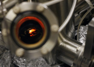
Unlock Microcontroller PIC18F4439 means the security fuse bits will be cut off by the FIB technique or laser beam during the process of MCU Crack
A Phase Locked Loop circuit is provided as a programmable option for users that want to multiply the frequency of the incoming crystal oscillator signal by 4. For an input clock frequency of 5 MHz, the internal clock frequency will be multiplied to 20 MHz. This is useful for customers who are concerned with EMI due to high frequency crystals.
The PLL can only be enabled when the oscillator configuration bits are programmed for HS mode. If they are programmed for any other mode, the PLL is not enabled and the system clock will come directly from OSC1.
The PLL is one of the modes specified by the FOSC<2:0> configuration bits. The Oscillator mode is specified during device programming. A PLL lock timer is used to ensure that the PLL has locked before device execution starts. The PLL lock timer has a time-out that is called TPLL.
When the device executes a SLEEP instruction, the oscillator is turned off and the device is held at the beginning of an instruction cycle (Q1 state). With the oscillator off, the OSC1 and OSC2 signals will stop oscillating. Since all the transistor switching currents have been removed, SLEEP mode achieves the lowest current consumption of the device (only leakage currents).
Enabling any on-chip feature that will operate during SLEEP will increase the current consumed during SLEEP. The user can wake from SLEEP through external RESET, Watchdog Timer Reset, or through an interrupt.
Power-up delays are controlled by two timers, so that no external RESET circuitry is required for most applications. The delays ensure that the device is kept in RESET, until the device power supply and clock are stable. For additional information on RESET operation, see Section 3.0.
The first timer is the Power-up Timer (PWRT), which optionally provides a fixed delay of 72 ms (nominal) on power-up only (POR and BOR). The second timer is the Oscillator Start-up Timer (OST), intended to keep the chip in RESET until the crystal oscillator is stable.
With the PLL enabled (HS/PLL Oscillator mode), the time-out sequence following a Power-on Reset is different from other Oscillator modes. The time-out sequence is as follows:
1. The PWRT time-out is invoked after a POR time delay has expired.
2. The Oscillator Start-up Timer (OST) is invoked. However, this is still not a sufficient amount of time to allow the PLL to lock at high frequencies. The PIC18FXX39 differentiates between various kinds of RESET:
a) Power-on Reset (POR)
b) MCLR Reset during normal operation
c) MCLR Reset during SLEEP
d) Watchdog Timer (WDT) Reset (during normal operation)
e) Programmable Brown-out Reset (BOR)
f) RESET Instruction
g) Stack Full Reset
h) Stack Underflow Reset
Most registers are unaffected by a RESET. Their status is unknown on POR and unchanged by all other RESETS. The other registers are forced to a “RESET state” on Power-on Reset, MCLR, WDT Reset, Brown-out Reset, MCLR Reset during SLEEP and by the RESET instruction.
Most registers are not affected by a WDT wake-up, since this is viewed as the resumption of normal operation . Status bits from the RCON register, RI, TO, PD, POR and BOR, are set or cleared differently in different RESET situations, as indicated in Table 3-2. These bits are used in software to determine the nature of the RESET. See Table 3-3 for a full description of the RESET states of all registers.
A simplified block diagram of the On-Chip Reset Circuit is shown in Figure 3-1.
The Enhanced MCU devices have a MCLR noise filter in the MCLR Reset path. The filter will detect and ignore small pulses.
The MCLR pin is not driven low by any internal RESETS, including the WDT.
Tags: unlock microcontroller flash archive,unlock microcontroller flash code,unlock microcontroller flash content,unlock microcontroller flash data,unlock microcontroller flash eeprom,unlock microcontroller flash file,unlock microcontroller flash firmware,unlock microcontroller flash information,unlock microcontroller flash memory,unlock microcontroller flash program
Related Products
-
Unlock ATMEL MCU ATMEGA48A Firmware
No. -

Unlock Microcontroller ATtiny261 Heximal
No. -

Unlock Microcontroller ATtiny4313A Heximal
No. -

Unlock Microcontroller ATtiny2313A Software
No. -

Unlock Microcontroller ATTINY2313 Binary
No. -

Unlock Microcontroller ATTINY85 Firmware
No. -

Unlock Microcontroller ATTINY45V Firmware
No.