-
Product Categories
Live Support Chat


Unlock Microcontroller ATmega64 Eeprom
Unlock Microcontroller ATmega64 Eeprom and dump its data out from it, and program from flash memory, by reverse engineering MCU circuitry pattern by decapsulate the silicon cover and get access to the internal structure;
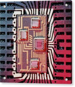
Unlock Microcontroller ATmega64 Eeprom and dump its data out from it, and program from flash memory, by reverse engineering MCU circuitry pattern by decapsulate the silicon cover and get access to the internal structure
The ATmega64 provides the following features: 64K bytes of In-System Programmable Flash with Unlock-While-Write capabilities, 2K bytes EEPROM, 4K bytes SRAM, 53 general purpose I/O lines, 32 general purpose working registers, Real Time Counter (RTC), four flexible Timer/Counters with compare modes and PWM, two USARTs, a byte oriented Two-wire Serial Interface, an 8-channel, 10-bit ADC with optional differential input stage with programmable gain, programmable Watchdog Timer with internal Oscillator, an SPI serial port, IEEE std. 1149.1 compliant JTAG test interface, also used for accessing the On-chip Debug system and programming, and six software selectable power saving modes when Microchip IC dsPIC30F3010 program cloning.
The Idle mode stops the CPU while allowing the SRAM, Timer/Counters, SPI port, and interrupt system to continue functioning. The Power down mode saves the register contents but freezes the Oscillator, disabling all other chip functions until the next interrupt or Hardware Reset if Microchip Microcomputer dsPIC33FJ128MC506 controller decoding.
In Power-save mode, the asynchronous timer continues to run, allowing the user to maintain a timer base while the rest of the device is sleeping. The ADC Noise Reduction mode stops the CPU and all I/O modules except asynchronous timer and ADC, to minimize switching noise during ADC conversions.
In Standby mode, the crystal/resonator Oscillator is running while the rest of the device is sleeping. This allows very fast start-up combined with low power consumption. In Extended Standby mode, both the main Oscillator and the asynchronous timer continue to run after ST ARM MCU STM8S103F3P3 unlocking.
The device is manufactured using Atmel’s high-density non-volatile memory technology. The On-chip ISP Flash allows the program memory to be reprogrammed In-System through an SPI serial interface, by a conventional non-volatile memory programmer, or by an On-chip Boot program running on the AVR core. The Boot Program can use any interface to download the Application Program in the Application Flash memory.
Software in the Boot Flash section will continue to run while the Application Flash section is updated, providing true Unlock-While-Write operation. By combining an 8-bit RISC CPU with In-System Self-Programmable Flash on a monolithic chip, the Atmel ATmega64 is a powerful microcontroller that provides a highly-flexible and cost-effective solution to many embedded control applications.
The ATmega64 AVR is supported with a full suite of program and system development tools including: C compilers, macro assemblers, program debugger/simulators, In-Circuit Emulators, and evaluation kits. The ATmega64 is a highly complex microcontroller where the number of I/O locations supersedes the 64 I/O location reserved in the AVR instruction set.
To ensure backward compatibility with the ATmega103, all I/O locations present in ATmega103 have the same location in ATmega64. Most additional I/O locations are added in an Extended I/O space starting from 0x60 to 0xFF (i.e., in the ATmega103 internal RAM space).
These location can be reached by using LD/LDS/LDD and ST/STS/STD instructions only, not by using IN and OUT instructions. The relocation of the internal RAM space may still be a problem for ATmega103 users. Also, the increased number of Interrupt Vectors might be a problem if the code uses absolute addresses. To solve these problems, an ATmega103 compatibility mode can be selected by programming the fuse M103C.
In this mode, none of the functions in the Extended I/O space are in use, so the internal RAM is located as in ATmega103. Also, the extended Interrupt Vectors are removed. The ATmega64 is 100% pin compatible with ATmega103, and can replace the ATmega103 on current printed circuit boards. The application notes “Replacing ATmega103 by ATmega128” and “Migration between ATmega64 and ATmega128” describes what the user should be aware of replacing the ATmega103 by an ATmega128 or ATmega64.
Tags: microcontroller source archive unlock,microcontroller source code unlock,microcontroller source content unlock,microcontroller source data unlock,microcontroller source eeprom unlock,microcontroller source file unlock,microcontroller source firmware unlock,microcontroller source information unlock,microcontroller source memory unlock,microcontroller source program unlock
