-
Product Categories
Live Support Chat


Unlock Microcontroller ATMEGA48V Program
Unlock Microcontroller ATMEGA48V and dump Program from flash and data from eeprom, the security fuse bit will be disable after decapsulate the MCU internal structure and cut it off by focus ion beam to read MCU firmware;
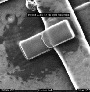
Unlock Microcontroller ATMEGA48V and dump Program from flash and data from eeprom, the security fuse bit will be disable after decapsulate the MCU internal structure and cut it off by focus ion beam to read MCU firmware
Port B is an 8-bit bi-directional I/O port with internal pull-up resistors (selected for each bit). The Port B output buffers have symmetrical drive characteristics with both high sink and source capability. As inputs, Port B pins that are externally pulled low will source current if the pull-up resistors are activated. The Port B pins are tri-stated when a reset condition becomes active, even if the clock is not running when read microcontroller pic18f6585 software.
Depending on the clock selection fuse settings, PB6 can be used as input to the inverting Oscillator amplifier and input to the internal clock operating circuit. Depending on the clock selection fuse settings, PB7 can be used as output from the inverting Oscillator amplifier.
If the Internal Calibrated RC Oscillator is used as chip clock source, PB7..6 is used as TOSC2..1 input for the Asynchronous Timer/Counter2 if the AS2 bit in ASSR is set before crack mcu pic18f8680 binary.
Port C is a 7-bit bi-directional I/O port with internal pull-up resistors (selected for each bit). The PC5..0 output buffers have symmetrical drive characteristics with both high sink and source capability. As inputs, Port C pins that are externally pulled low will source current if the pull-up resistors are activated. The Port C pins are tri-stated when a reset condition becomes active, even if the clock is not running.
If the RSTDISBL Fuse is programmed, PC6 is used as an I/O pin. Note that the electrical characteristics of PC6 differ from those of the other pins of Port C. If the RSTDISBL Fuse is unprogrammed, PC6 is used as a Reset input. A low level on this pin for longer than the minimum pulse length will generate a Reset, even if the clock is not running.
Port D is an 8-bit bi-directional I/O port with internal pull-up resistors (selected for each bit). The Port D output buffers have symmetrical drive characteristics with both high sink and source capability. As inputs, Port D pins that are externally pulled low will source current if the pull-up resistors are activated. The Port D pins are tri-stated when a reset condition becomes active, even if the clock is not running.
AVCC is the supply voltage pin for the A/D Converter, PC3:0, and ADC7:6. It should be externally connected to VCC, even if the ADC is not used. If the ADC is used, it should be connected to VCC through a low-pass filter. Note that PC6..4 use digital supply voltage, VCC.
In the TQFP and QFN/MLF package, ADC7:6 serve as analog inputs to the A/D converter. These pins are powered from the analog supply and serve as 10-bit ADC channels. The ATmega48/88/168 is a low-power CMOS 8-bit microcontroller based on the AVR enhanced RISC architecture.
By executing powerful instructions in a single clock cycle, the ATmega48/88/168 achieves throughputs approaching 1 MIPS per MHz allowing the system designer to optimize power consumption versus processing speed.
Tags: microcontroller dump archive unlocking,microcontroller dump code unlocking,microcontroller dump content unlocking,microcontroller dump data unlocking,microcontroller dump eeprom unlocking,microcontroller dump file unlocking,microcontroller dump firmware unlocking,microcontroller dump information unlocking,microcontroller dump memory unlocking,microcontroller dump program unlocking
