-
Product Categories
Live Support Chat


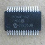
Unlock Microcontroller ATmega2560V Heximal
Unlock Microcontroller ATmega2560V encrypted memory and readout the heximal from its flash and eeprom, copy the firmware into other blank MCU ATmega2560V which will provide the same functions;
Unlock Microcontroller ATmega2560V encrypted memory and readout the heximal from its flash and eeprom, copy the firmware into other blank MCU ATmega2560V which will provide the same functions
The ATmega2560V AVR is supported with a full suite of program and system development tools including: C Compilers, Macro Assemblers, Program Debugger/Simulators, In-Circuit Emulators, and Evaluation kits.
The ATMEGA2560V differ only in memory sizes, boot loader support, and interrupt vector sizes. Table 2-1 summarizes the different memory and interrupt vector sizes for the devices.
ATMEGA2560V support a real Read-While-Write Self-Programming mechanism. There is a separate Boot Loader Section, and the SPM instruction can only execute from there.
In ATMEGA2560V there is no Read-While-Write support and no separate Boot Loader Section. The SPM instruction can execute from the entire Flash.
1. For compatibility with future devices, reserved bits should be written to zero if accessed. Reserved I/O memory addresses should never be written.
2. I/O Registers within the address range 0x00 – 0x1F are directly bit-accessible using the SBI and CBI instructions. In these registers, the value of single bits can be checked by using the SBIS and SBIC instructions.
3. Some of the Status Flags are cleared by writing a logical one to them. Note that, unlike most other AVRs, the CBI and SBI instructions will only operate on the specified bit, and can therefore be used on registers containing such Status Flags. The CBI and SBI instructions work with registers 0x00 to 0x1F only to faciliate the IC breaking procedures.
4. When using the I/O specific commands IN and OUT, the I/O addresses 0x00 – 0x3F must be used. When addressing I/O Registers as data space using LD and ST instructions, 0x20 must be added to these addresses.
The ATMEGA2560V is a complex microcontroller with more peripheral units than can be supported within the 64 location reserved in Opcode for the IN and OUT instructions. For the Extended I/O space from 0x60 – 0xFF in SRAM, only the ST/STS/STD and LD/LDS/LDD instructions can be used.
5. Only valid for ATMEGA2560V.
6. BODS and BODSE only available for picoPower devices ATMEGA2560V.
Tags: unlock microcontroller protected archive,unlock microcontroller protected bin,unlock microcontroller protected code,unlock microcontroller protected content,unlock microcontroller protected data,unlock microcontroller protected eeprom,unlock microcontroller protected file,unlock microcontroller protected firmware,unlock microcontroller protected hex,unlock microcontroller protected information,unlock microcontroller protected memory,unlock microcontroller protected program