-
Product Categories
Live Support Chat


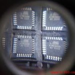
Unlock Microcontroller ATmega1280PA Binary
Unlock Microcontroller ATmega1280PA encrypted program memory for embedded MCU ATmega1280PA binary extraction, security fuse bit can be found through reverse engineering microprocessor ATmega1280PA:
On ATtiny15L, PB5 is input or open-drain output. Because this pin is used for 12V programming, there is no ESD protection diode limiting the voltage on the pin to VCC + 0.5V.
Thus, special care should be taken to ensure that the voltage on this pin does not rise above VCC + 1V during normal operation. This may cause the MCU to reset or enter programming mode unintentionally if unlock microcontroller at89c51rc2 eeprom.
All Port B pins are connected to a pin change detector that can trigger the pin change interrupt. See “Pin Change Interrupt” on page 21 for details.
When the RSTDISBL fuse is unprogrammed, this pin serves as External Reset. When the RSTDISBL fuse is programmed, this pin is a general input pin or a open-drain output pin. If DDB5 is cleared (zero), PB5 is configured as an input pin. If DDB5 is set (one), the pin is a open-drain output after unlock microcontroller at89c51rd2 flash.
- SCK/INT0/T0 – PORT B, Bit 2
In Serial Programming mode, this pin serves as the serial clock input, SCK. In normal mode, this pin can serve as the external interrupt0 input. See the interrupt description for details on how to enable this interrupt. Note that activity on this pin will trigger the interrupt even if the pin is configured as an output.
In normal mode, this pin can serve as the external counter clock input. See the Timer/Counter0 description for further details. If external Timer/Counter clocking is selected, activity on this pin will clock the counter even if it is configured as an output.
In Serial Programming mode, this pin serves as the serial data output, MISO. In normal mode, this pin can serve as Timer/Counter1 output compare match output (OC1A) before unlock chip at89c5130a flash.
See the Timer/Counter1 description for further details, and how to enable the output. The OC1A pin is also the output pin for PWM mode timer function. This pin also serves as the negative input of the On-chip Analog Comparator.
Tags: unlock microcontroller software archive,unlock microcontroller software binary,unlock microcontroller software code,unlock microcontroller software content,unlock microcontroller software data,unlock microcontroller software eeprom,unlock microcontroller software file,unlock microcontroller software firmware,unlock microcontroller software heximal,unlock microcontroller software information,unlock microcontroller software memory,unlock microcontroller software program