-
Product Categories
Live Support Chat


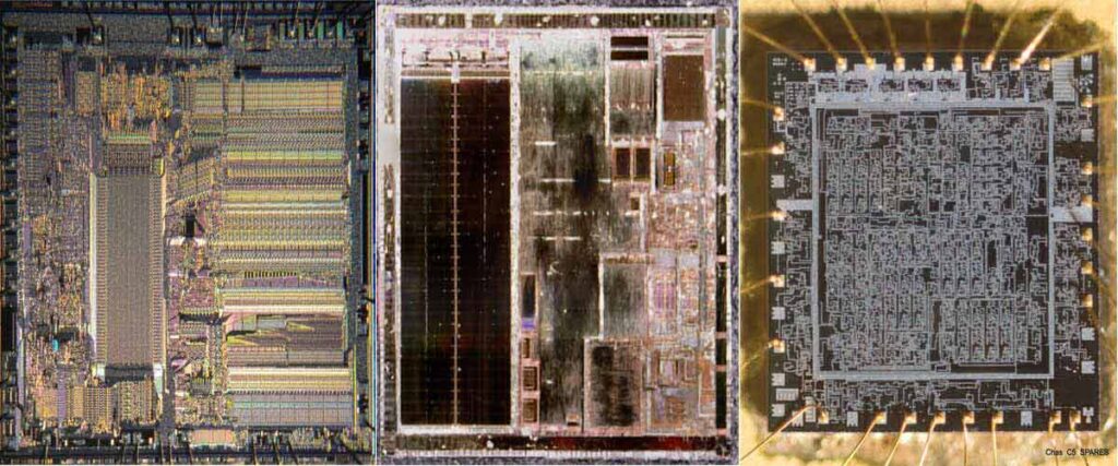
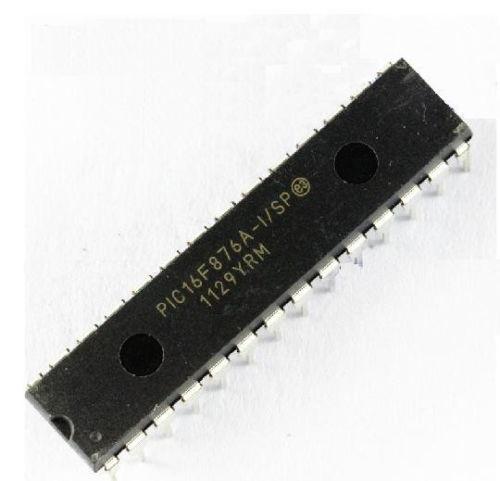
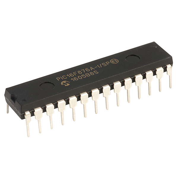
Unlock Microchip MCU PIC16F876 Binary
Unlock Microchip MCU PIC16F876 starts from break microcontroller pic16f876 fuse bit protection and then readout protective binary from pic16f876 flash and eeprom memory;
MEMORY ORGANIZATION
There are three memory blocks in each of the PIC16F87X MCUs. The Program Memory and Data Memory have separate buses so that concurrent access can occur and is detailed in this section. The EEPROM data memory block is detailed in Section 4.0. Additional information on device memory may be found in the PICmicro Mid-Range Reference Manual, (DS33023) when discover texas instrument msp430f2131 MCU.
Program Memory Organization
The PIC16F87X devices have a 13-bit program counter capable of addressing an 8K x 14 program memory space. The PIC16F877/876 devices have 8K x 14 words of FLASH program memory, and the PIC16F873/874 devices have 4K x 14. Accessing a location above the physically implemented address will cause a wraparound. The RESET vector is at 0000h and the interrupt vector is at 0004h.
DATA MEMORY ORGANIZATION
The data memory is partitioned into multiple banks which contain the General Purpose Registers and the Special Function Registers. Bits RP1 (STATUS<6>) and RP0 (STATUS<5>) are the bank select bits.
Each bank extends up to 7Fh (128 bytes). The lower Locations of each bank are reserved for the Special Function Registers. Above the Special Function Registers are General Purpose Registers, implemented as static RAM. All implemented banks contain Special Function Registers. Some frequently used Special Function Registers from one bank may be mirrored in another bank for code reduction and quicker access.
SPECIAL FUNCTION REGISTER
The Special Function Registers are registers used by the CPU and peripheral modules for controlling the desired operation of the device. These registers are implemented as static RAM.
The Special Function Registers can be classified into two sets: core (CPU) and peripheral. Those registers associated with the core functions are described in detail in this section. Those related to the operation of the peripheral features are described in detail in the peripheral features section.