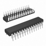
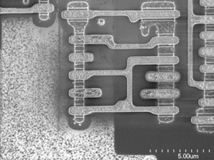
Unlock MCU ATTINY48 Program
Unlock MCU ATTINY48 Program from its flash memory, use laser to cut off the security fuse bit and disable its protective system, ATtiny48 Microcontroller can be reversed through decapsulated and get access to the internal structure of the MCU;
Unlock MCU ATTINY48 Program from its flash memory, use laser to cut off the security fuse bit and disable its protective system, ATtiny48 Microcontroller can be reversed through decapsulated
Port K is a 8-bit bi-directional I/O port with internal pull-up resistors (selected for each bit). The Port K output buffers have symmetrical drive characteristics with both high sink and source capability.
As inputs, Port K pins that are externally pulled low will source current if the pull-up resistors are activated. The Port K pins are tri-stated when a reset condition becomes active, even if the clock is not running if crack mcu pic12f510 program.
Port L is a 8-bit bi-directional I/O port with internal pull-up resistors (selected for each bit). The Port L output buffers have symmetrical drive characteristics with both high sink and source capability.
As inputs, Port L pins that are externally pulled low will source current if the pull-up resistors are activated. The Port L pins are tri-stated when a reset condition becomes active, even if the clock is not running after unlock mcu program.
Reset input. A low level on this pin for longer than the minimum pulse length will generate a reset, even if the clock is not running. The minimum pulse length is given in Table 23 on page 58. Shorter pulses are not guaranteed to generate a reset when unlock ic pic16f57 program.
Input to the inverting Oscillator amplifier and input to the internal clock operating circuit. Output from the inverting Oscillator amplifier. AVCC is the supply voltage pin for Port F and the A/D Converter.
It should be externally connected to VCC, even if the ADC is not used. If the ADC is used, it should be connected to VCC through a low-pass filter.
This is the analog reference pin for the A/D Converter. This documentation contains simple code examples that briefly show how to use various parts of the device. Be aware that not all C compiler vendors include bit definitions in the header files and interrupt handling in C is compiler dependent after unlock microcontroller pic16f627a bin.
Please confirm with the C compiler documentation for more details. These code examples assume that the part specific header file is included before compilation. For I/O registers located in extended I/O map, “IN”, “OUT”, “SBIS”, “SBIC”, “CBI”, and “SBI” instructions must be replaced with instructions that allow access to extended I/O. Typically “LDS” and “STS” combined with “SBRS”, “SBRC”, “SBR”, and “CBR”.
Tags: unlock mcu archive,unlock mcu bin,unlock mcu code,unlock mcu content,unlock mcu data,unlock mcu eeprom,unlock mcu file,unlock mcu firmware,unlock mcu hex,unlock mcu information,unlock mcu memory,unlock mcu program