-
Product Categories
Live Support Chat


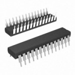
Unlock MCU ATmega2560A Heximal
Unlock MCU ATmega2560A memory needs to reverse engineering microcontroller ATmega2560, and locate the security fuse bit in the Microprocessor by cutting it off by focus ion beam, replicate Heximal to new MCU;
Unlock MCU ATmega2560A memory needs to reverse engineering microcontroller ATmega2560, and locate the security fuse bit in the Microprocessor by cutting it off by focus ion beam, replicate Heximal to new MCU
The AT89S53 features DATA Polling to indicate the end of a write cycle. During a write cycle in the parallel or serial programming mode, an attempted read of the last byte written will result in the complement of the written datum on P0.7 (parallel mode), and on the MSB of the serial output byte on MISO (serial mode).
Once the write cycle has been completed, true data are valid on all outputs, and the next cycle may begin. DATA Polling may begin any time after a write cycle has been initiated by unlocking Microcontroller PIC12C509A binary.
The progress of byte programming in the parallel programming mode can also be monitored by the RDY/BSY output signal. Pin P3.4 is pulled Low after ALE goes High during programming to indicate BUSY.
P3.4 is pulled High again when programming is done to indicate READY. If lock bits LB1 and LB2 have not been programmed, the programmed Code can be read back via the address and data lines for verification. The state of the lock bits can also be verified directly in the parallel programming mode.
In the serial programming mode, the state of the lock bits can only be verified indirectly by observing that the lock bit features are enabled. In the parallel programming mode, chip erase is initiated by using the proper combination of control signals and by holding ALE/PROG low for 10 ms.
The Code array is written with all “1”s in the Chip Erase operation. In the serial programming mode, a chip erase operation is initiated by issuing the Chip Erase instruction. In this mode, chip erase is self-timed and takes about 16 ms. During chip erase, a serial read from any address location will return 00H at the data outputs in the process of reading MCU PIC16F689 software.
A programmable fuse is available to disable Serial Programming if the user needs maximum system security. The Serial Programming Fuse can only be programmed or erased in the Parallel Programming Mode.
Tags: unlock mcu archive,unlock mcu binary,unlock mcu code,unlock mcu content,unlock mcu data,unlock mcu eeprom,unlock mcu file,unlock mcu firmware,unlock mcu heximal,unlock mcu information,unlock mcu memory,unlock mcu program