-
Product Categories
Live Support Chat


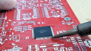
Unlock MCU AT89C5131 Code
Unlock MCU AT89C5131 encrypted memory, readout the code from its memory which include flash and eeprom, rewrite the firmware into other blank Microcontroller AT89C5131 in the format of heximal or binary by universal programmer as MCU recovery;
Unlock MCU AT89C5131 encrypted memory, readout the code from its memory which include flash and eeprom, rewrite the firmware into other blank Microcontroller AT89C5131 in the format of heximal or binary by universal programmer
These security bits protect the code access through the parallel programming interface. They are set by default to level 4. The code access through the ISP is still possible and is controlled by the “software security bits” which are stored in the extra Flash memory accessed by the ISP firmware when MCU PIC16F628 firmware extraction.
To load a new application with the parallel programmer, a chip erase must be done first. This will set the HSB in its inactive state and will erase the Flash memory. The part reference can always be read using Flash parallel programming modes.
The default value of the HSB provides parts ready to be programmed with ISP:
BLJB: Cleared to force ISP operation.
X2: Set to force X1 mode (Standard Mode)
OSCON1-0: Set to start with 32 MHz oscillator configuration value.
LB2-0: Security level four to protect the code from a parallel access with maximum security.
Software Registers
Several registers are used, in factory and by parallel programmers, to make copies of hardware registers contents. These values are used by Atmel ISP (see Section “In-System Programming (ISP)”). These registers are in the “Extra Flash Memory” part of the Flash memory. This block is also called ”XAF” or eXtra Array Flash. They are accessed in the following ways:
Commands issued by the parallel memory programmer.
Commands issued by the ISP software.
Calls of API issued by the application software.
Several software registers are described in Table 39.
In the AT89C5131, the lowest 16K or 32K of the 64 Kbyte program memory address space is filled by internal Flash. When the EA is pin high, the processor fetches instructions from internal program Flash. Bus expansion for accessing program memory from 16K or 32K upward is automatic since external instruction fetches occur automatically when the program counter exceeds 3FFFh (16K) or 7FFFh (32K) if Unlock MCU. If the EA pin is tied low, all program memory fetches are from external memory. If all storage is on chip, then byte location 3FFFh (16K) or 7FFFh (32K) should be left vacant to prevent and undesired pre-fetch from external program memory address 4000h (16K) or 8000h (32K) when Unlock chip PIC16HV616 eeprom.
The 1-Kbyte on-chip EEPROM memory block is located at addresses 0000h to 03FFh of the ERAM memory space and is selected by setting control bits in the EECON register before Unlock MCU. A read in the EEPROM memory is done with a MOVX instruction. A physical write in the EEPROM memory is done in two steps: write data in the column latches and transfer of all data latches into an EEPROM memory row (programming).
The number of data written on the page may vary from 1 to 128 bytes (the page size). When programming, only the data written in the column latch is programmed and a ninth bit is used to obtain this feature. This provides the capability to program the whole memory by bytes, by page or by a number of bytes in a page. Indeed, each ninth bit is set when the writing the corresponding byte in a row and all these ninth bits are reset after the writing of the complete EEPROM row.
Tags: unlock mcu heximal archive,unlock mcu heximal code,unlock mcu heximal content,unlock mcu heximal data,unlock mcu heximal eeprom,unlock mcu heximal file,unlock mcu heximal firmware,unlock mcu heximal information,unlock mcu heximal memory,unlock mcu heximal program


